Microstrip antenna for RFID device

Inactive Publication Date: 2007-07-19
UNIVERSITY OF KANSAS
View PDF18 Cites 247 Cited by
  • Summary
  • Abstract
  • Description
  • Claims
  • Application Information

AI Technical Summary

Benefits of technology

[0015] The present invention overcomes the above-described and other problems by providing an improved microstrip patch antenna, feed structure, and matching circuit for an RFID tag, including a balanced feed design, a dual feed structure design, a combined ne

Problems solved by technology

However, typical antennas used in near-field systems are typically only a small fraction of a wavelength in their linear dimensions and, therefore, are inefficient electromagnetic radiators and receptors.
As a result, the useful range of operation may be limited to as little as a few inches from the interrogator antenna.
Such a short read distance is a significant disadvantage in many applications.
However, compared to the HF band, the radiation and reception of EM waves at these higher frequency bands are affected much more strongly by obstacles and materials in the immediate environment of the antennas.
In particular, attaching tags to metal objects or containers containing metal or water is problematic.
However, dipole antennas suffer considerable performance degradation when placed near a high-loss and/or high-dielectric material, such as water, or near a conductor, such as metal.
This is commonly referred to as the “metal/water problem” and occurs because the dielectric material changes the electromagnetic properties of the antenna, which changes the resonant frequency and efficiency of the antenna.
More specifically, when a dipole antenna is placed near a conductor, the operation of the antenna changes from that of a “free space resonator” to a “volume resonator”, which impacts the performance of the a

Method used


Image

  • Microstrip antenna for RFID device
  • Microstrip antenna for RFID device
  • Microstrip antenna for RFID device

Examples


Embodiment Construction

, below.

BRIEF DESCRIPTION OF THE DRAWINGS

[0023] The following drawings form part of the present specification and are included to further demonstrate certain aspects of the present invention. The figures are examples only, and do not limit the scope of the invention.

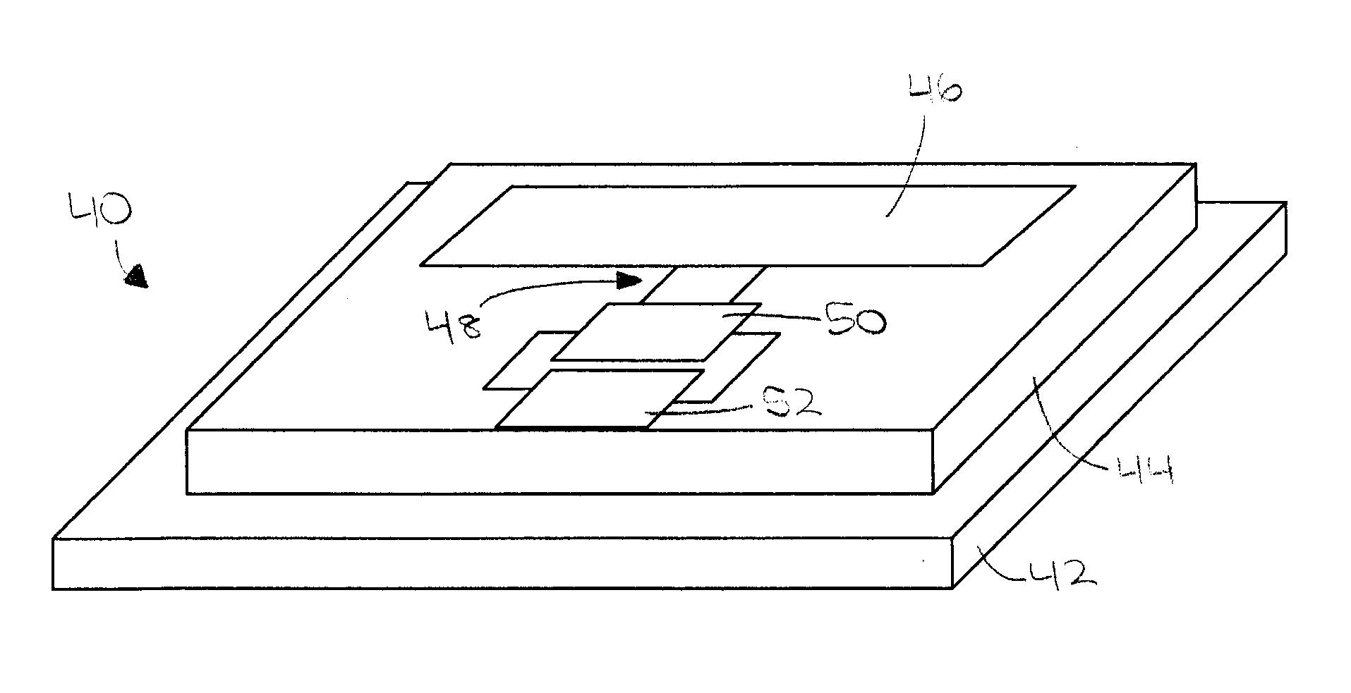
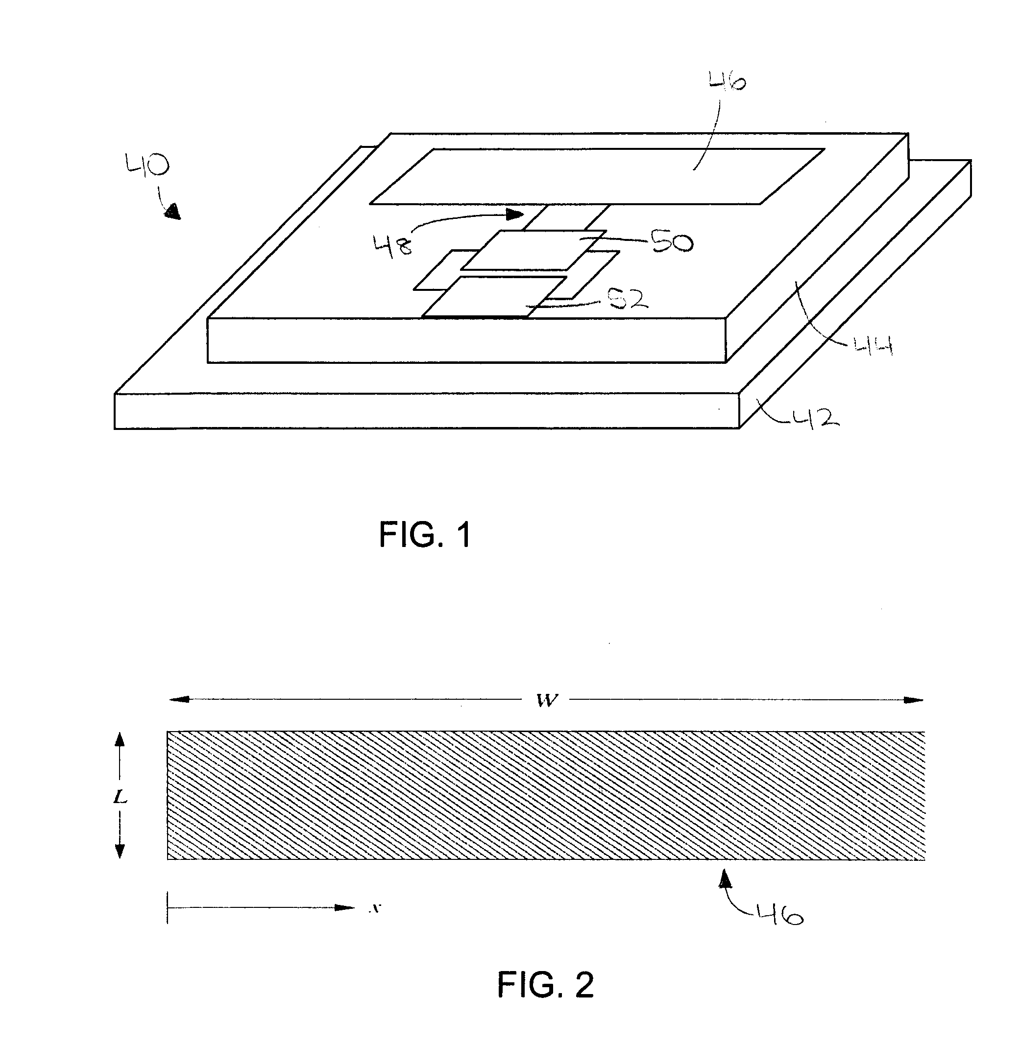
[0024]FIG. 1 is an isometric view of a model RFID tag to which the improvements of the present invention can be applied.

[0025]FIG. 2 is a plan view of a model microstrip antenna such as may be used in implementing the improvements of the present invention.

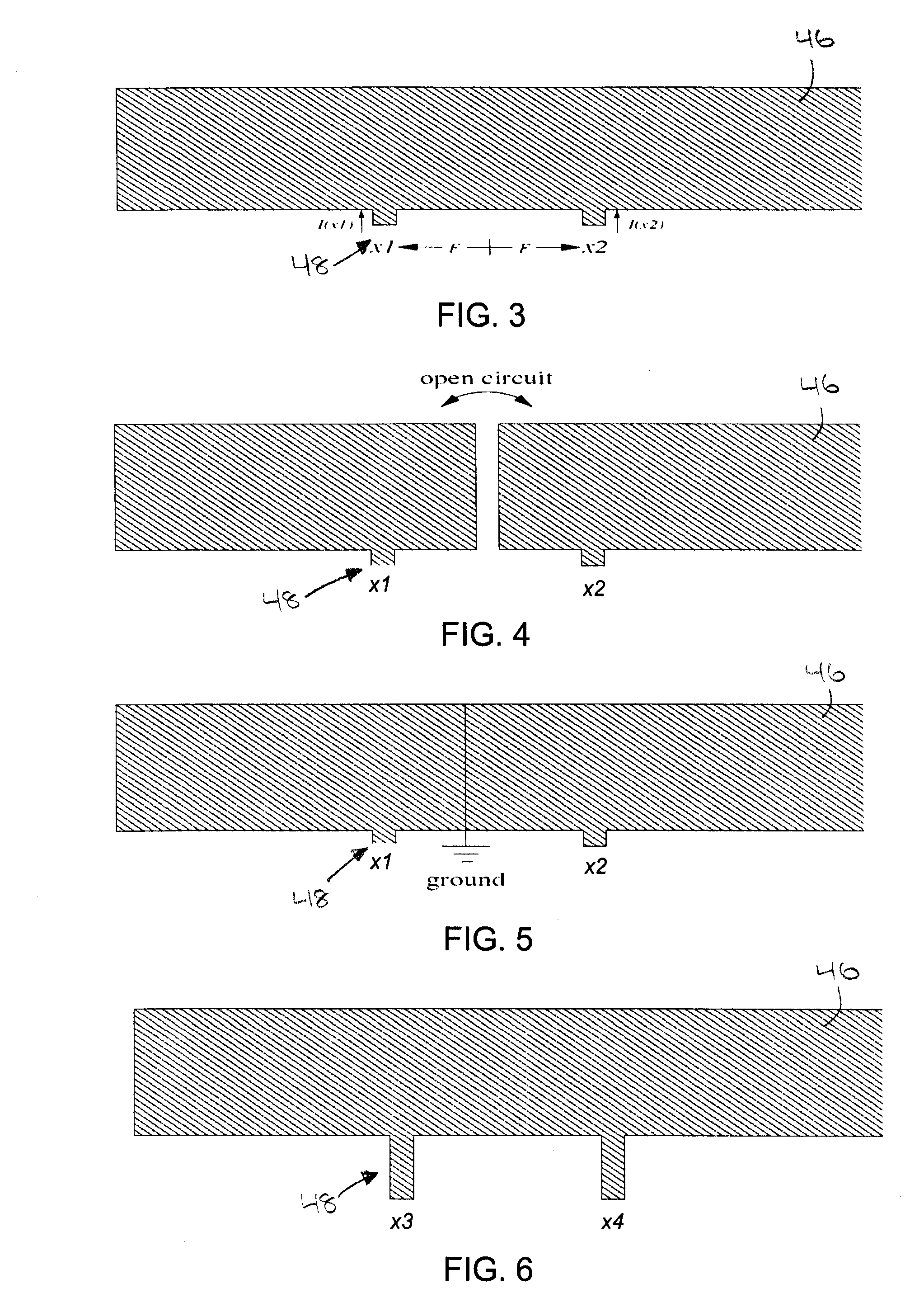
[0026]FIG. 3 is a plan view of the microstrip antenna having first and second feed structures.

[0027]FIG. 4 is a plan view of the microstrip antenna having first and second balanced feed structures driven in an even mode.

[0028]FIG. 5 is a plan view of the microstrip antenna having first and second balanced feed structures driven in an odd mode.

[0029]FIG. 6 is a plan view of the microstrip antenna having first and second balanced feed structures which have been ext...


PUM


Abstract

Microstrip patch antenna (46), feed structure (48), and matching circuit (50) designs for an RFID tag (10). A balanced feed design using balanced feeds coupled by a shorting stub (56) to create a virtual short between the two feeds so as to eliminate the need for physically connecting substrate to the ground plane. A dual feed structure design using a four-terminal IC can be connected to two antennas (46a,46b) resonating at different frequencies so as to provide directional and polarization diversity. A combined near/field-far/field design using a microstrip antenna providing electromagnetic coupling for far-field operation, and a looping matching circuit providing inductive coupling for near-field operation. A dual-antenna design using first and second microstrip antennas providing directional diversity when affixed to a cylindrical or conical object, and a protective superstrate (66). An annual antenna (46c) design for application to the top of a metal cylinder around a stem.

Description

RELATED APPLICATIONS [0001] The present non-provisional patent application is related to and claims priority benefit of an earlier-filed provisional patent application titled RADIO FREQUENCY IDENTIFICATION (RFID) ANTENNA TECHNIQUES, Ser. No. 60 / 750,182, filed Dec. 14, 2005. The identified earlier-filed application is hereby incorporated by reference into the present application.FIELD OF THE INVENTION [0002] The present invention relates generally to radio frequency identification (RFID) devices, and, more specifically, to microstrip patch antennas for RFID devices and methods for making same. BACKGROUND OF THE INVENTION [0003] RFID devices are used in a variety of different applications, including, for example, monitoring, cataloging, and tracking items. An RFID system typically includes a transponder, or “tag”, for storing and transmitting data, an interrogator, or “reader”, for receiving the data from the tag, and a data communications network for conveying the data received by th...

Claims


Application Information

Patent Timeline
IPC IPC(8): G08B13/14H01Q9/04
CPCG06K19/07749H01Q5/40H01Q1/22H01Q1/2208H01Q1/2216H01Q1/2225H01Q1/38H01Q1/48H01Q9/0407H01Q9/0442H01Q9/28H01Q9/30H01Q9/40H01Q23/00H01Q5/35G06K19/07786
Inventor DEAVOURS, DANIEL D.SIVAKUMAR, MUTHARASU
Owner UNIVERSITY OF KANSAS
Why Eureka
Try Eureka