Nitride semiconductor device

a semiconductor device and nitride technology, applied in the field of nitride semiconductor devices, can solve the problems of difficulty in increasing the drain operation current, difficulty in obtaining enhancement characteristics, and difficulty in previously increasing the concentration of electrons generated in channels, etc., and achieve the effect of allowing the operation current to increas

Active Publication Date: 2007-07-26
PANASONIC CORP
View PDF6 Cites 19 Cited by
  • Summary
  • Abstract
  • Description
  • Claims
  • Application Information

AI Technical Summary

Benefits of technology

[0023]It is therefore an object of the present invention to provide a normally-OFF

Problems solved by technology

Accordingly, the resultant FET is likely to be of a depletion type (normally-ON type) and it is difficult to obtain characteristics of an enhancement type (normally-ON type).
However, if a JFET is of a normally-OFF type, it is difficult to previously increase the concentration of electrons generated in channel even by applying a forward bias to the gate electrode.
Therefore, a conventional JFET has the problem of difficulty in increasing drain operation current.
This causes electrons in the same amount as the holes to be generated in the channel region, thus obtaining large opera

Method used


Image

  • Nitride semiconductor device
  • Nitride semiconductor device
  • Nitride semiconductor device

Examples


embodiment 1

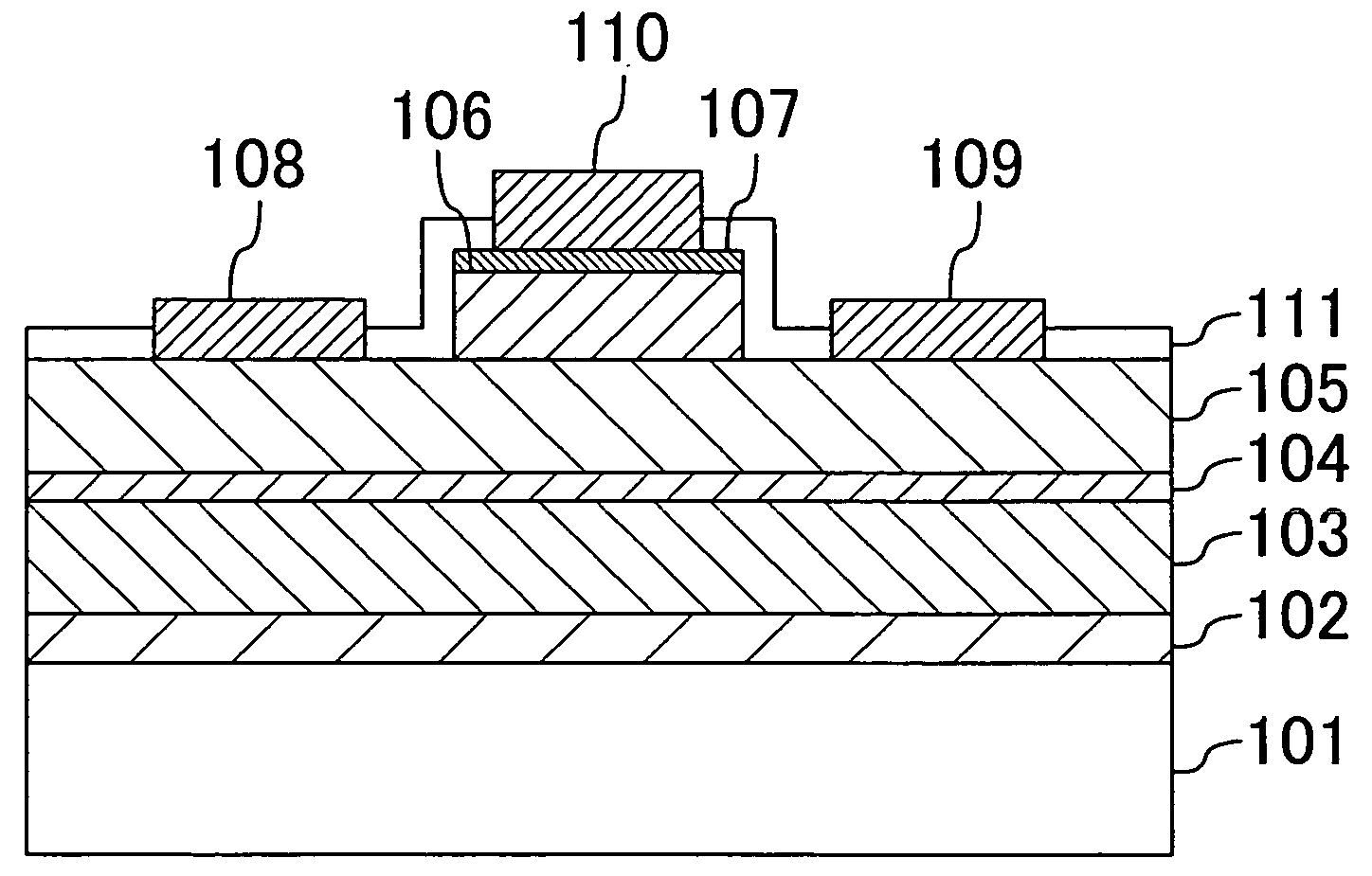
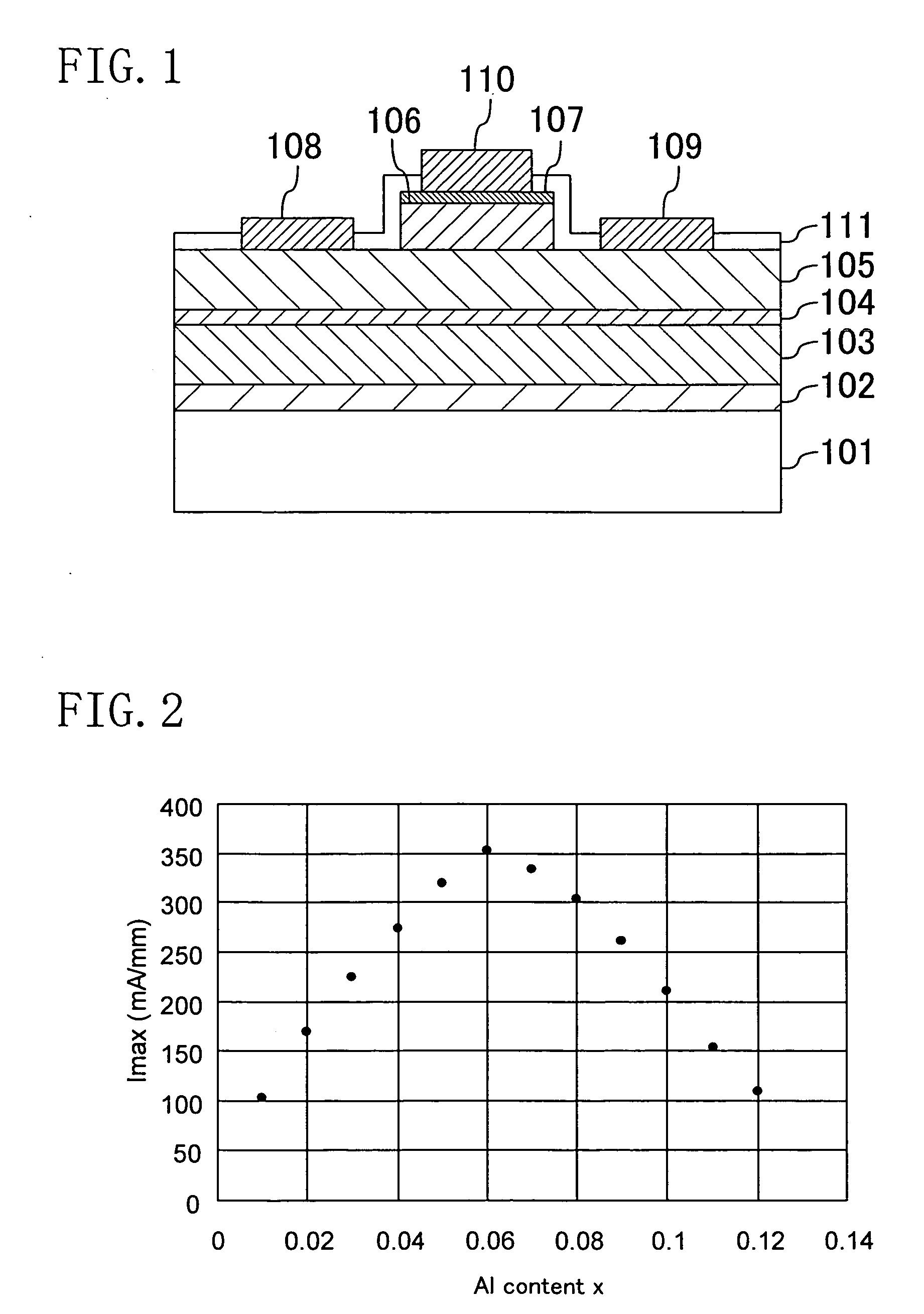
[0047]FIG. 1 illustrates an example of a cross-sectional structure of a nitride semiconductor device according to a first embodiment of the present invention.

[0048]As illustrated in FIG. 1, a transistor which is the nitride semiconductor device of this embodiment includes: a sapphire (Al2O3) substrate 101 having a principal surface whose surface orientation is a (0001) plane; a AlN buffer layer 102 formed on the substrate 101 and having a thickness of 100 nm; an underlying layer 103 formed on the buffer layer 102, having a thickness of 1 μm and made of undoped AlxGa1-xN (where 0104 formed on the underlying layer 103, having a thickness of 3.5 nm and made of undoped GaN; a second semiconductor layer 105 formed on the first semiconductor layer 104, having a thickness of 25 nm and made of undoped Al0.15Ga0.85N; a control layer 106 formed on the second semiconductor layer 105, having a thickness of 100 nm and made of p-type Al0.15Ga0.85N; and a contact layer 107 formed on the control la...

embodiment 2

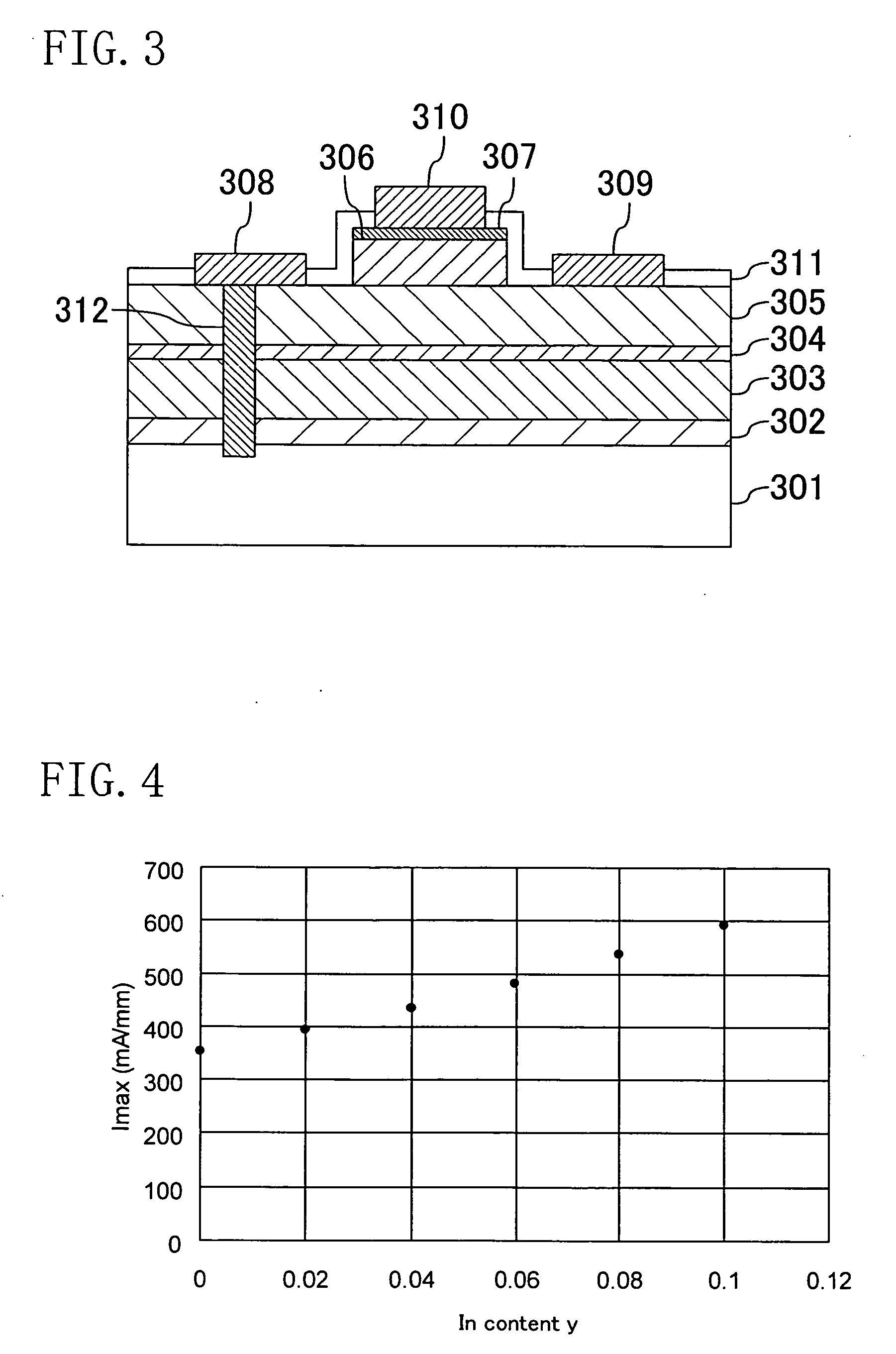
[0059]FIG. 3 illustrates an example of a cross-sectional structure of a nitride semiconductor device according to a second embodiment of the present invention.

[0060]As illustrated in FIG. 3, a transistor which is the nitride semiconductor device of this embodiment includes: an n-type Si substrate 301 having a principal surface whose surface orientation is a (111) plane; a buffer layer 302 formed on the substrate 301, having a thickness of 40 nm and made of AlN; an underlying layer 303 formed on the buffer layer 302, having a thickness of 1 μm and made of undoped Al0.05Ga0.95N; a first semiconductor layer 304 formed on the underlying layer 303, having a thickness of 3.5 nm and made of undoped InyGa1-yN (where 0305 formed on the first semiconductor layer 304, having a thickness of 25 nm and made of undoped Al0.15Ga0.85N; a control layer 306 formed on the second semiconductor layer 305, having a thickness of 100 nm and made of p-type Al0.15Ga0.85N; and a contact layer 307 formed on the...

embodiment 3

[0066]FIG. 5 illustrates an example of a cross-sectional structure of a nitride semiconductor device according to a third embodiment of the present invention.

[0067]As illustrated in FIG. 5, a transistor which is the nitride semiconductor device of this embodiment includes: a sapphire substrate 501 having a principal surface whose surface orientation is a (0001) plane; a buffer layer 502 formed on the substrate 501, having a thickness of 100 nm and made of AlN; an underlying layer 503 formed on the buffer layer 502, having a thickness of 1 μm and made of undoped Al0.05Ga0.95N; a first semiconductor layer 504 formed on the underlying layer 503, having a thickness of 3.5 nm and made of undoped GaN; a second semiconductor layer 505 formed on the first semiconductor layer 504, having a thickness of 25 nm and made of undoped Al0.15Ga0.85N; a control layer 506 formed on the second semiconductor layer 505, having a thickness of 100 nm and made of p-type Al0.15Ga0.85N; and a contact layer 50...


PUM


Abstract

A nitride semiconductor device includes: a first semiconductor layer made of first nitride semiconductor; a second semiconductor layer formed on a principal surface of the first semiconductor layer and made of second nitride semiconductor having a bandgap wider than that of the first nitride semiconductor; a control layer selectively formed on, or above, an upper portion of the second semiconductor layer and made of third nitride semiconductor having a p-type conductivity; source and drain electrodes formed on the second semiconductor layer at respective sides of the control layer; a gate electrode formed on the control layer; and a fourth semiconductor layer formed on a surface of the first semiconductor layer opposite to the principal surface, having a potential barrier in a valence band with respect to the first nitride semiconductor and made of fourth nitride semiconductor containing aluminum.

Description

CROSS-REFERENCE TO RELATED APPLICATION[0001]The disclosure of Japanese Patent Application No. 2006-016622 filed in Japan on Jan. 25, 2006 including specification, drawings and claims is incorporated herein by reference in its entirety.BACKGROUND OF THE INVENTION[0002]The present invention relates to nitride semiconductor devices made of Group III-V nitride semiconductor containing gallium nitride (GaN) as a main component and capable of operating at positive voltages (normally-OFF operation).[0003]In recent years, field effect transistors (hereinafter, referred to as FETs) using GaN-based compound semiconductor materials have been intensively studied as radio-frequency (RF) high-power devices. Nitride semiconductor materials such as GaN enable formation of various mixed crystals together with aluminum nitride (AlN) or indium nitride (InN), and thus are capable of forming heterojunctions in the same manner as conventionally-used arsenic-based semiconductor materials containing galliu...

Claims


Application Information

Patent Timeline
IPC IPC(8): H01L31/00
CPCH01L21/02381H01L21/0242H01L21/02458H01L21/02502H01L21/0254H01L29/7787H01L29/2003H01L29/4175H01L29/432H01L29/452H01L29/7783H01L29/1066
Inventor UENO, HIROAKIYANAGIHARA, MANABUUEDA, TETSUZOUEMOTO, YASUHIROTANAKA, TSUYOSHIUEDA, DAISUKE
Owner PANASONIC CORP
Why Eureka
Try Eureka