
Structure and method for enhanced triple well latchup robustness

a technology of triple wells and latchups, applied in the direction of semiconductor devices, electrical devices, transistors, etc., can solve the problems of cmos latchup elimination and spacing problems, and achieve the effect of improving latchup robustness within the devi

Active Publication Date: 2007-07-26
TAIWAN SEMICON MFG CO LTD
View PDF24 Cites 13 Cited by
  • Summary
  • Abstract
  • Description
  • Claims
  • Application Information

AI Technical Summary

Benefits of technology

[0007] Thus, all three of the above-described embodiments of the invention address the issue of latchup by adding the second semiconductor layer (e.g., n+ layer) not only beneath the second semiconductor well (e.g., the p-well ) but also beneath the first semiconductor well (e.g., the n-well). This n+ layer degrades the vertical pnp device lowering the vertical bipolar current gain of the pnp and reducing series shunt resistance of pnpn by lowering the n-well contact to p+ device resistance (i.e., the effective n-well shunt resistance). Additionally, all three of these embodiments eliminate the spacing issues by extending the n+ layer and address n-channel MOSFET threshold voltage scattering by providing the p+ layer.
[0008] Each of these embodiments of the device can also comprise an isolation structure (e.g., a trench isolation structure (TI) or a deep trench isolation structure (DT)) within the device that extends from a top surface of the device to below an upper surface of the second semiconductor layer such that it eliminates lateral devices and, thereby, improves latchup robustness. The isolation structure can either bifurcate the first semiconductor well or can separate the first semiconductor well from the second semiconductor well. If the isolation structure separates the first and second semiconductor wells, then that portion of the second semiconductor layer below the second semiconductor well must abut the isolation structure to ensure that the second semiconductor well is isolated from the substrate.
[0010] Lastly, each of these embodiments of the device can also comprise a sub-collector region having the second conductivity type between the first semiconductor well and the second semiconductor layer. The sub-collector region comprises a higher concentration of a second conductivity type dopant than either the first semiconductor well or the second semiconductor layer and further improves latchup robustness.
[0013] Additionally, the method can comprise forming an isolation structure that extends from a top surface of the device to below an upper surface of the second semiconductor layer so as to eliminate lateral devices and, thereby, improve latchup robustness. The isolation structure can be formed to bifurcate the first semiconductor well. Alternatively, the isolation structure can be formed to separate the first semiconductor well and the second semiconductor well. However, if the isolation structure separates the first and second semiconductor wells, it must further be formed such that a portion of the second semiconductor layer below the second semiconductor well abuts the isolation structure in order to isolate the second semiconductor well from the substrate. This isolation structure can be formed as either a trench isolation structure (TI) that extends from the top surface of the device to below the upper surface of the second semiconductor layer but above the level of the first semiconductor layer. Alternatively, this isolation structure can be formed as a deep trench isolation structure (DT) that extends from the top surface of device into the substrate below the level of the first semiconductor layer.
[0015] To further improve latchup robustness within the device, the method can comprise before forming the first semiconductor well, forming a sub-collector region with the second conductivity type above one side of the second semiconductor layer and then, forming the first semiconductor well above the sub-collector region.

Problems solved by technology

Both noise isolation and the elimination of CMOS latchup are significant issues in advanced complementary metal oxide semiconductor (CMOS) technology and bipolar CMOS (BiCMOS) Silicon Germanium (SiGe) technology.
Additionally, because the buried n+ layer must overlap the n-wells in order to isolate the p-well, spacing issues present a problem in the current triple well CMOS formation process.

Method used


Image

  • Structure and method for enhanced triple well latchup robustness
  • Structure and method for enhanced triple well latchup robustness
  • Structure and method for enhanced triple well latchup robustness

Examples


Embodiment Construction

[0031] The embodiments of the invention and the various features and advantageous details thereof are explained more fully with reference to the non-limiting embodiments that are illustrated in the accompanying drawings and detailed in the following description. It should be noted that the features illustrated in the drawings are not necessarily drawn to scale. Descriptions of well-known components and processing techniques are omitted so as to not unnecessarily obscure the embodiments of the invention. The examples used herein are intended merely to facilitate an understanding of ways in which the embodiments of the invention may be practiced and to further enable those of skill in the art to practice the embodiments of the invention. Accordingly, the examples should not be construed as limiting the scope of the embodiments of the invention.

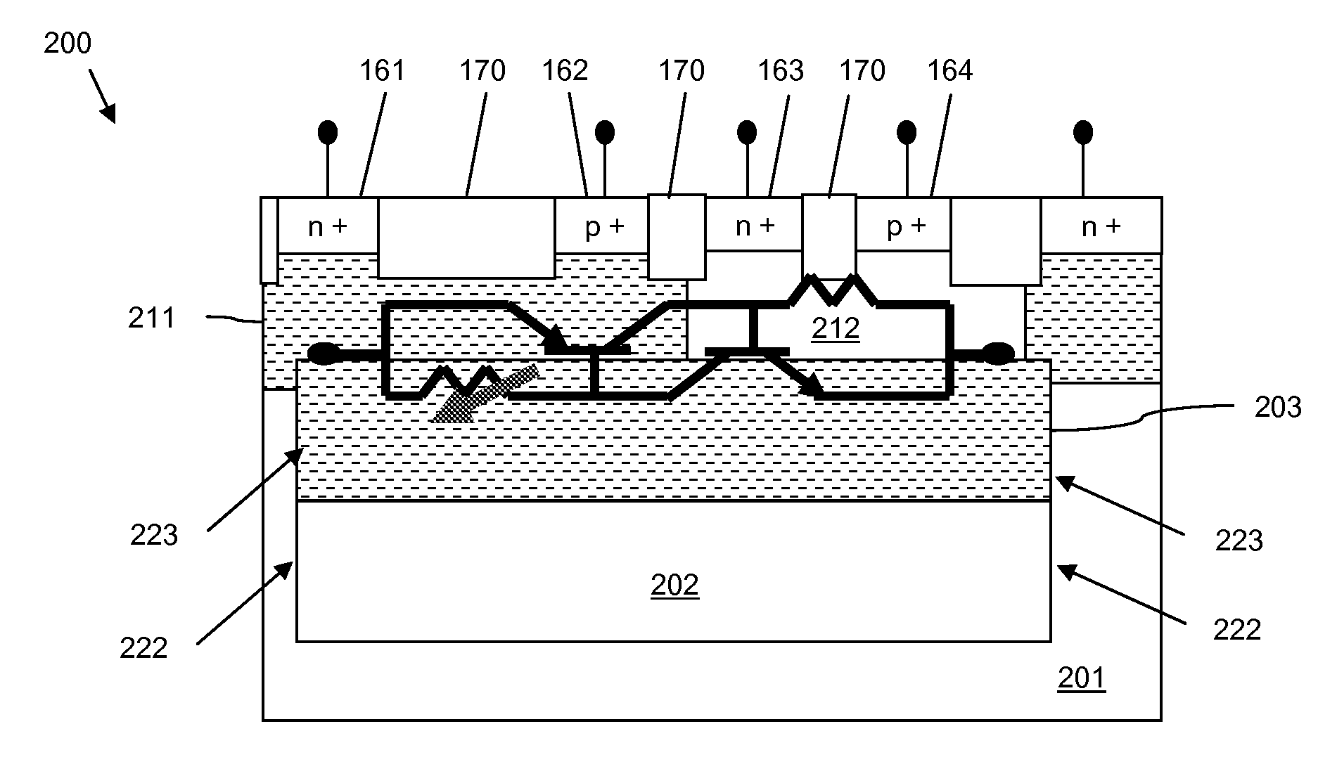
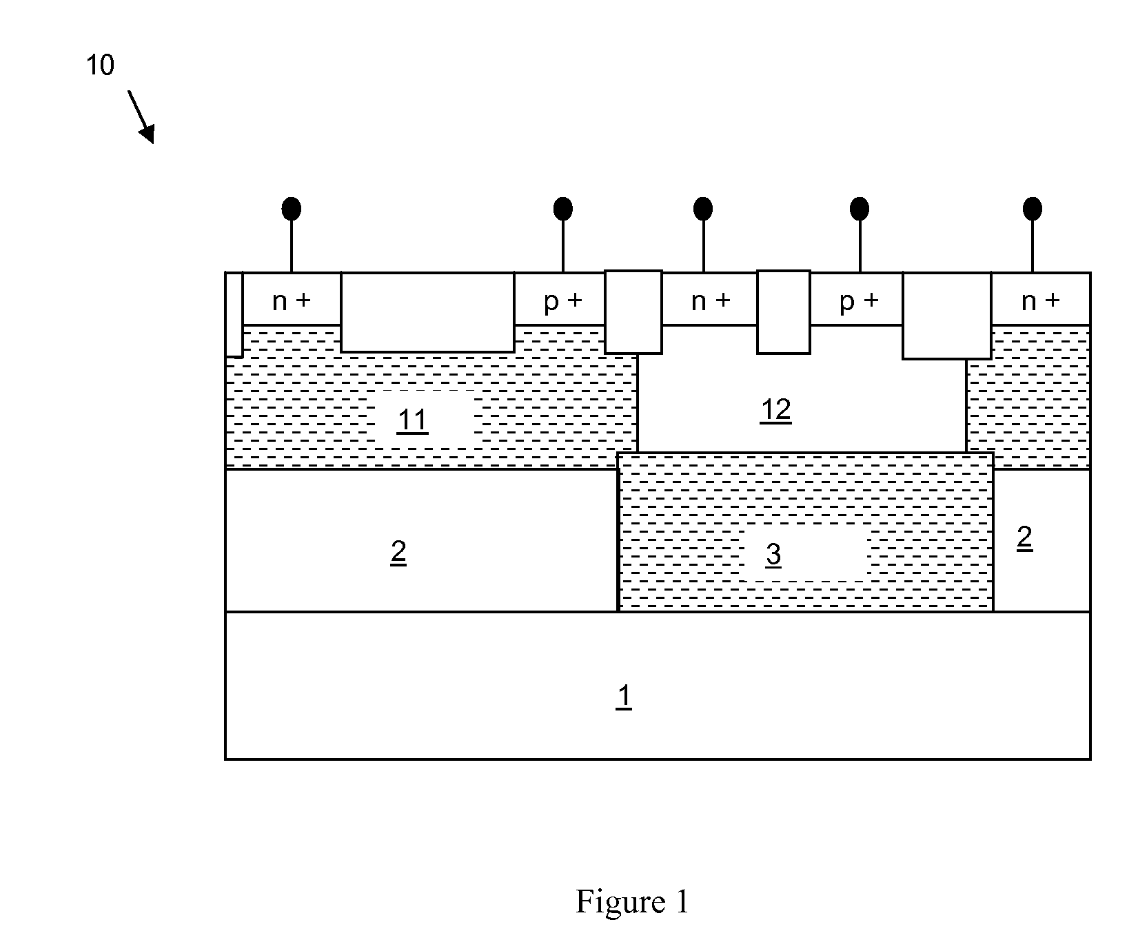
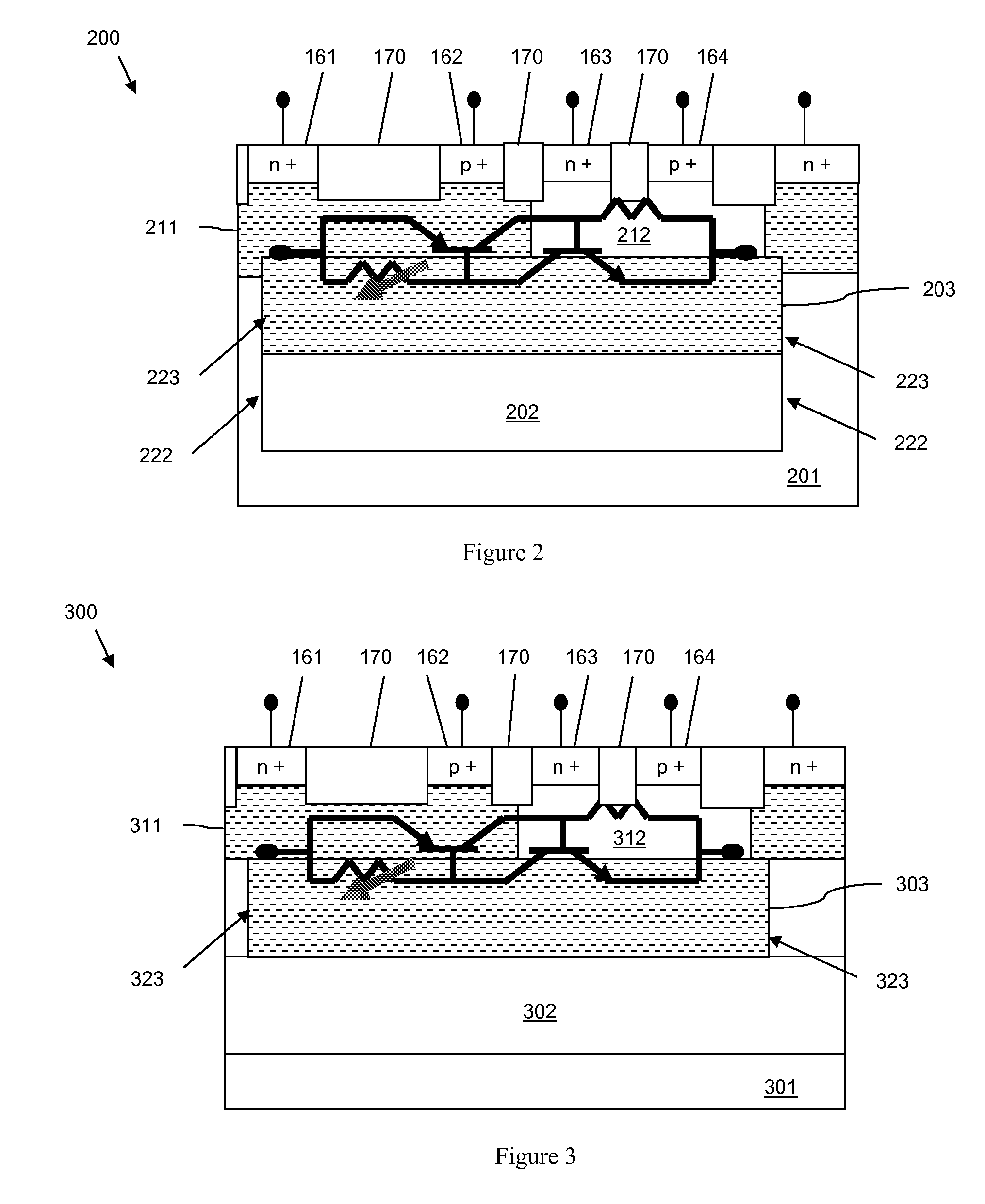
[0032] As mentioned above, and referring to FIG. 1, CMOS devices 10 that are formed using current state of the art triple well technology typi...


PUM


Abstract

Disclosed is a triple well CMOS device structure that addresses the issue of latchup by adding an n+ buried layer not only beneath the p-well to isolate the p-well from the p− substrate but also beneath the n-well. The structure eliminates the spacing issues between the n-well and n+ buried layer by extending the n+ buried layer below the entire device. The structure also addresses the issue of threshold voltage scattering by providing a p+ buried layer below the entire device under the n+ buried layer or below the p-well side of the device only either under or above the n+ buried layer) Latchup robustness can further be improved by incorporating into the device an isolation structure that eliminates lateral pnp, npn, or pnpn devices and / or a sub-collector region between the n+ buried layer and the n-well.

Description

BACKGROUND [0001] 1. Field of the Invention [0002] The embodiments of the invention generally relate to metal oxide semiconductor field effect transistor (MOSFET) devices, and, more particularly, to triple well technology in such MOSFET devices. [0003] 2. Description of the Related Art [0004] Both noise isolation and the elimination of CMOS latchup are significant issues in advanced complementary metal oxide semiconductor (CMOS) technology and bipolar CMOS (BiCMOS) Silicon Germanium (SiGe) technology. More particularly, as MOSFET threshold voltages decrease, the need to isolate circuitry from noise sources becomes more important and has lead to an increased interest in “isolated MOSFETs” (i.e., triple well technology). In current triple well technology, a buried n-type layer (i.e., a buried n+ layer) is placed below the p-well and a buried p-type layer (i.e., a p+ layer) is placed below the n-well (or n-well / sub-collector combinations) at the same level, but not displaced. The burie...

Claims


Application Information

Patent Timeline
Patent Type & Authority Applications(United States)
IPC IPC(8): H01L29/76H01L21/8238
CPCH01L21/761H01L29/1087H01L27/0928H01L27/0921
Inventor COLLINS, DAVID S.SLINKMAN, JAMES A.VOLDMAN, STEVEN H.
Owner TAIWAN SEMICON MFG CO LTD
Learn More