Product including conductor made of zinc or zinc aluminum alloy

a technology of zinc aluminum alloy and conductor, which is applied in the field of products, can solve the problems of unintentional melting of solder alloy, shortening the operating time of filling the minute through holes, and low melting point of solder alloy

Inactive Publication Date: 2007-07-26
FUJITSU LTD
View PDF12 Cites 7 Cited by
  • Summary
  • Abstract
  • Description
  • Claims
  • Application Information

AI Technical Summary

Benefits of technology

[0020] The addition of aluminum enables establishment of a thinner oxide film at the surface of the conductor made of the Zn—Al alloy. When the wiring is connected to the conductor in an oxygen-free atmosphere, electric conduction can reliably be established between the conductor and the wiring.

Problems solved by technology

However, since the melting point of the solder alloy is relatively low, the solder alloy unintentionally melts at a later stage where the package printed wiring board is to be mounted on a printed circuit board, for example.
However, the electroless copper plating suffers from a longer operating time for filling the minute through holes.
This leads to a lower production efficiency.

Method used


Image

  • Product including conductor made of zinc or zinc aluminum alloy
  • Product including conductor made of zinc or zinc aluminum alloy
  • Product including conductor made of zinc or zinc aluminum alloy

Examples


Embodiment Construction

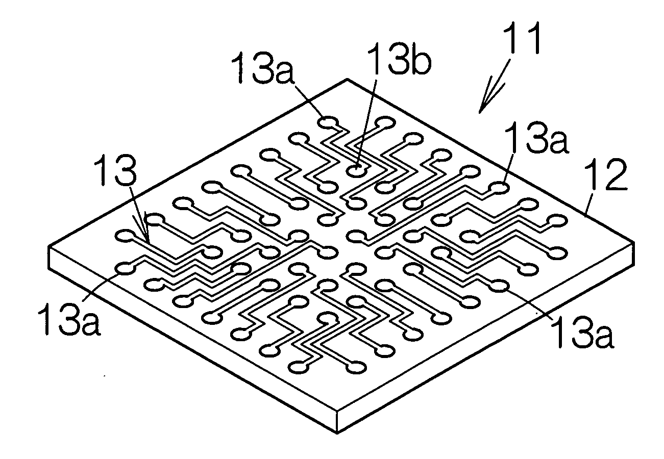
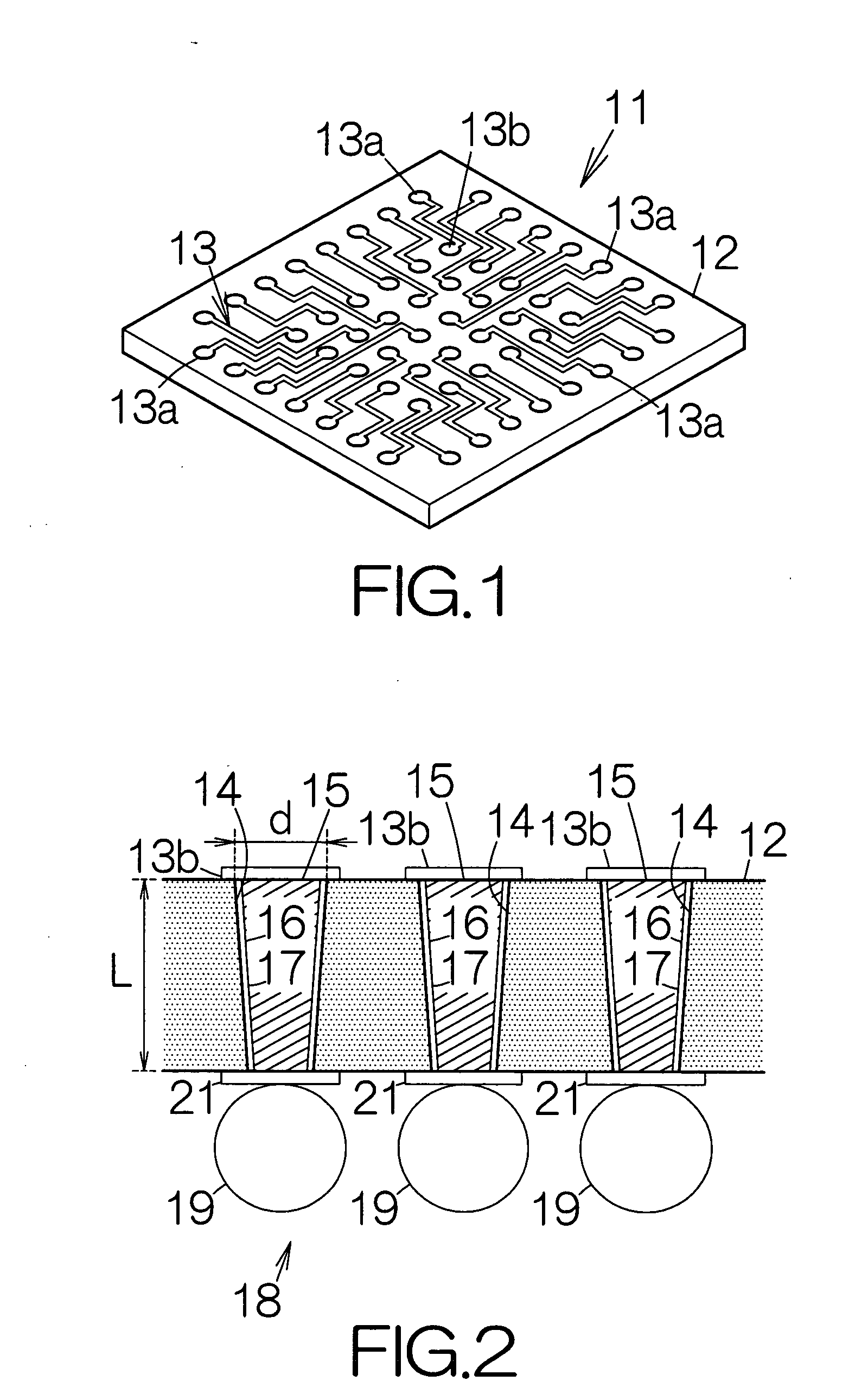
[0034]FIG. 1 schematically illustrates a package printed wiring board 11 according to a first embodiment of the present invention. The package printed wiring board 11 includes a glass substrate 12. A wiring pattern 13 is formed on the front surface of the glass substrate 12. The wiring pattern 13 is made of an electrically-conductive material such as aluminum or copper. Pads 13a, 13b are defined in the wiring pattern 13, for example. The pads 13a are located on the glass substrate 12 along the outer periphery of the glass substrate 12. The pads 13b are located at positions in an area inside the rows of the pads 13a. The package printed wiring board 11 may employ an inorganic substrate such as a silicon substrate or a ceramic substrate in place of the glass substrate 12. It should be noted that the glass substrate 12 may have any thickness. Here, the thickness of the glass substrate 12 is set at 400 μm approximately, for example.

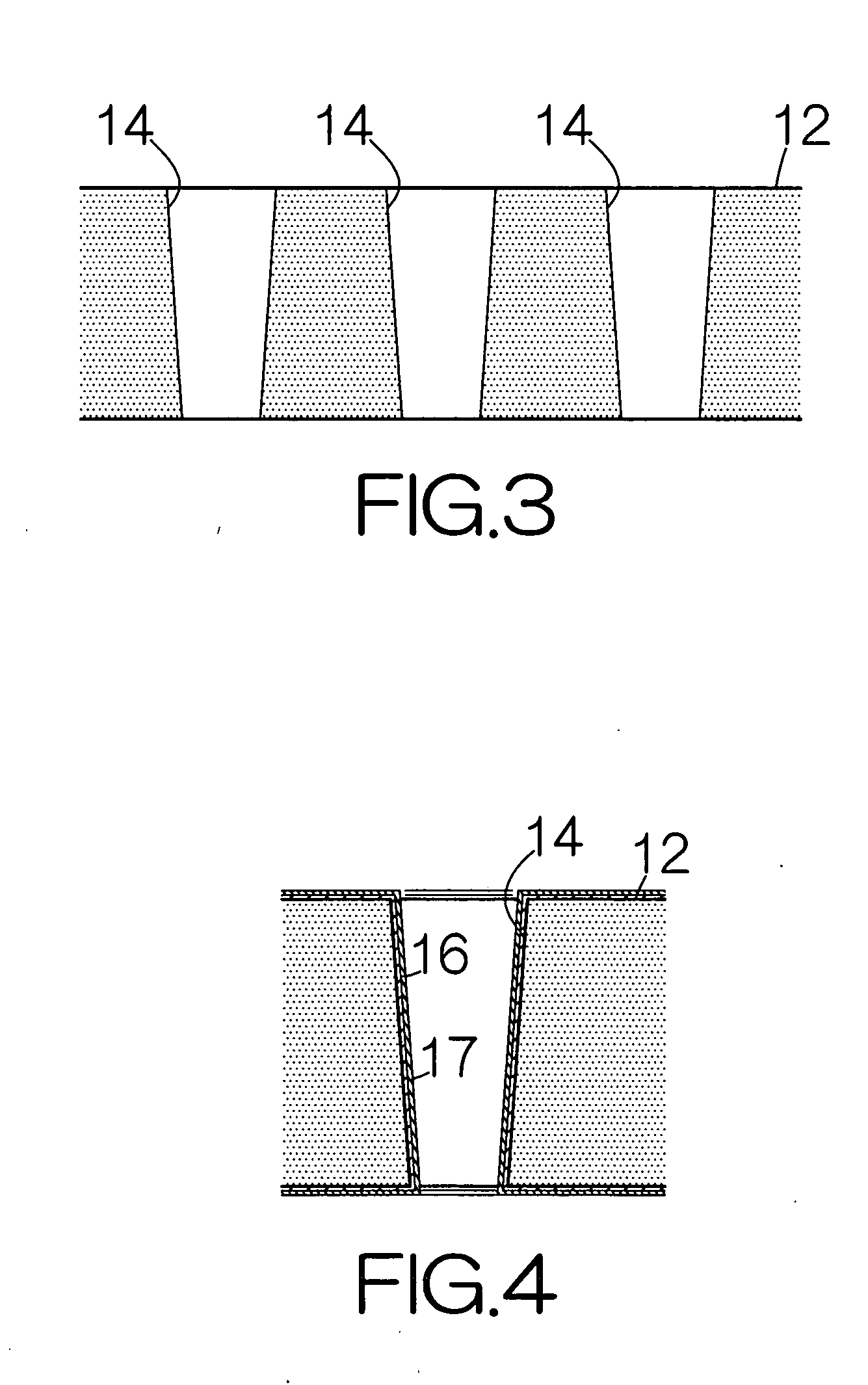
[0035] As shown in FIG. 2, through holes 14 are formed...


PUM

PropertyMeasurementUnit
aspect ratioaaaaaaaaaa
temperatureaaaaaaaaaa

Abstract

A hole is defined in a body of a product. A conductor made of zinc or a Zn—Al alloy fills the hole. Zinc or the Zn—Al alloy melts at a temperature equal to or higher than 375 degrees Celsius. Molten Zinc or Zn—Al alloy reliably fills the hole. Zinc and Zn—Al alloy have an electric conductivity. The hole can reliably be filled up with a conductor. The product reliably remains solid even when the product is secondarily exposed to a heat causing a solder alloy to melt. If Zn—Al alloy is utilized in the product, the Zn—Al alloy preferably contains aluminum at a content equal to or smaller than 1.0 weight %. The melting point of such a Zn—Al alloy can be kept equal to or higher than 400 degrees Celsius. The Zn—Al alloy can thus remain solid during a high temperature treatment such as anodic bonding.

Description

BACKGROUND OF THE INVENTION [0001] 1. Field of the Invention [0002] The present invention relates to a product, a material, and the like, including a body and a conductor filling a hole defined in the body. In particular, the present invention relates to a printed wiring board employing the product. [0003] 2. Description of the Prior Art [0004] Consideration is given to formation of a so-called through hole in a small-sized package printed wiring board. The through hole of the small-sized printed wiring board has a larger aspect ratio and a smaller inside diameter as compared with the through hole of a general large-sized printed wiring board. The inside of the through hole must be filled up with a conductor so as to avoid a larger increase in the electric resistance of the through hole. [0005] A through hole can be filled with a solder alloy as described in Japanese Patent Application Publication No. 2002-43751. However, since the melting point of the solder alloy is relatively low...

Claims


Application Information

Patent Timeline
Patent Type & Authority Applications(United States)
IPC IPC(8): H01L23/48
CPCH01L23/49827Y10T29/49165H01L2224/16H01L2924/01078H01L2924/01079H01L2924/09701H01L2924/15311H05K1/0306H05K3/4038H05K3/426H05K2203/128H01L2924/01327H01L23/49866Y10T29/49155H01L2924/00
Inventor KITAJIMA, MASAYUKIMATSUYAMA, RYOJI
Owner FUJITSU LTD
Why Eureka
Try Eureka