Active device array substrate, liquid crystal display panel and examining methods thereof

Inactive Publication Date: 2007-07-26
CHUNGHWA PICTURE TUBES LTD
View PDF8 Cites 14 Cited by
  • Summary
  • Abstract
  • Description
  • Claims
  • Application Information

AI Technical Summary

Benefits of technology

[0010] Accordingly, an object of the present invention is to

Problems solved by technology

However, the rising “environmental protection” awareness against its power consumption and radiation disadvantage, and its limited flattening capability against the market demands of light, thin, short, small, chic, and power-saving displays, have limited the growing space of CRTs.
It should be noted that, the examining circuit is complicated, and may reduce the layout region on the panel.
In addition, electrostatic accumulation may occur in the liquid crystal display panel, due to external

Method used


Image

  • Active device array substrate, liquid crystal display panel and examining methods thereof
  • Active device array substrate, liquid crystal display panel and examining methods thereof
  • Active device array substrate, liquid crystal display panel and examining methods thereof

Examples


Embodiment Construction

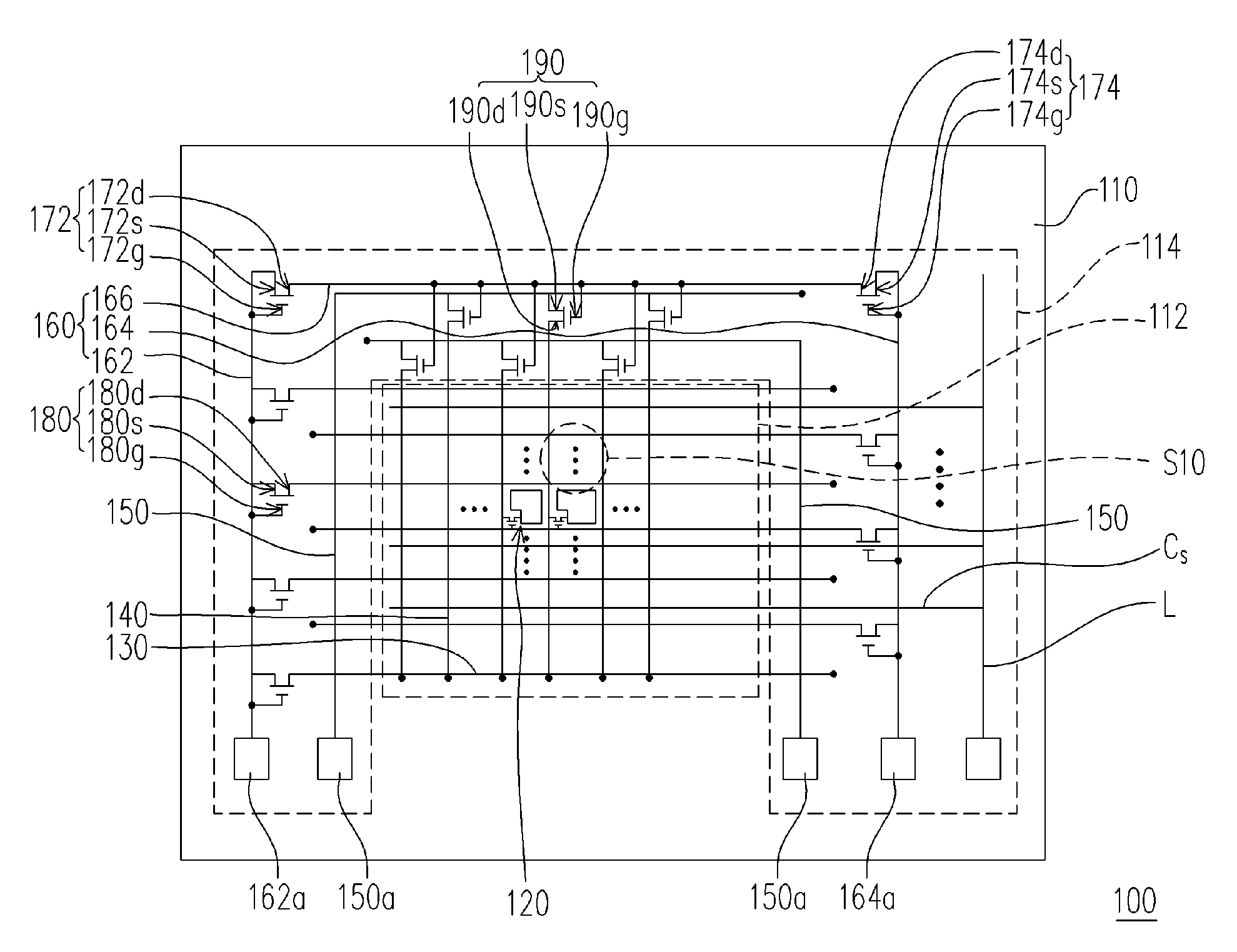
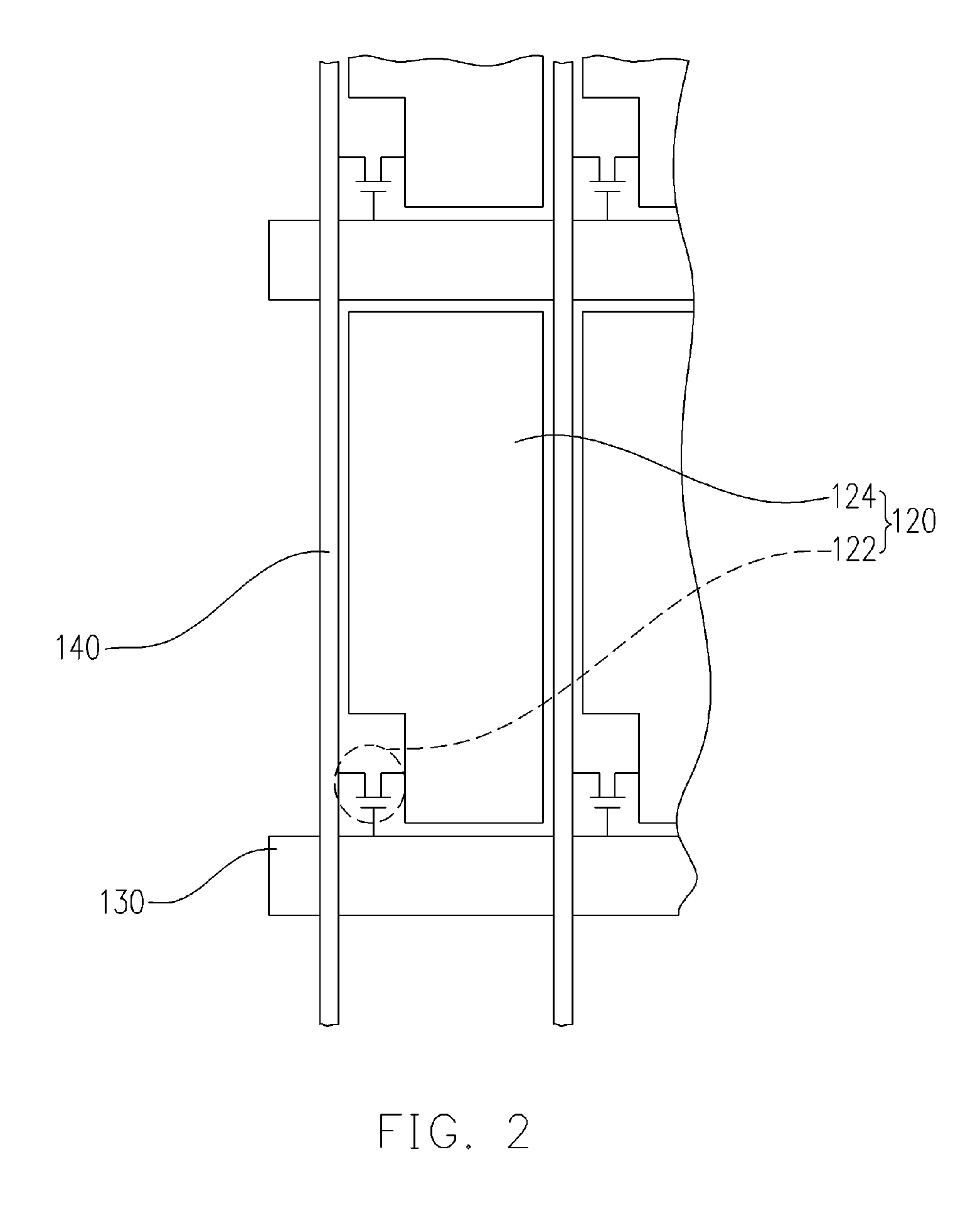
[0037]FIG. 1 shows a structural view of an active device array substrate according to a preferred embodiment of the present invention. Referring to FIG. 1, an active device array substrate 100 comprises a substrate 110, pixel units 120, scan lines 130, data lines 140, two data testing lines 150, an inner short ring 160, a first active device 172, a second active device 174, third active devices 180 and fourth active devices 190.

[0038] The substrate 110 can be a glass substrate, a quartz substrate or a substrate made of other suitable materials, and has an adjacent display region 112 and a peripheral circuit region 114. The pixel units 120 are disposed in the display region 112. The scan lines 130 can be aluminum alloy wires or wires made of other suitable conductive materials. And the data lines 140 can be chromium metal wires, aluminum alloy wires or wires made of other suitable conductive materials. The scan lines 130 and the data lines 140 are both disposed on the substrate 110 ...


PUM


Abstract

Pixel units are disposed in a display region of a substrate, and scan lines and data lines are used to control the pixel units. Inner short ring includes a first segment, a second segment and a connecting segment connecting both segments. The gates and sources of the first and second active device connect with the first and second segments respectively, and the drains connect with the connecting segment. The gates and sources of part of the third active devices connect with the first segment, and the drains connect with the odd scan lines. The gates and sources of other third active devices connect with the second segment, and the drains connect with the even scan lines. The gates of the fourth active devices connect with connecting lines, and the sources connect with data testing lines, and the drains connect with the odd and even data lines respectively.

Description

BACKGROUND OF THE INVENTION [0001] 1. Field of Invention [0002] The present invention relates to an active device array substrate, a display panel and examining methods thereof. More particularly, the present invention relates to an active device array substrate, a liquid crystal display panel having an inner short ring and examining methods thereof. [0003] 2. Description of Related Art [0004] In response to the increasing demand of the display, the industry put efforts in the development of the display. Among the displays, the cathode ray tube (CRT) has occupied the display market for many years, due to its high display quality and mature technology. However, the rising “environmental protection” awareness against its power consumption and radiation disadvantage, and its limited flattening capability against the market demands of light, thin, short, small, chic, and power-saving displays, have limited the growing space of CRTs. Therefore, the thin film transistor liquid crystal dis...

Claims


Application Information

Patent Timeline
IPC IPC(8): G01R31/00
CPCG02F2001/136254G02F1/136204G02F1/136254
Inventor CHANG, YUAN-HAOHUANG, CHIN-HAILIN, KUANG-HSIANG
Owner CHUNGHWA PICTURE TUBES LTD
Why Eureka
Try Eureka