

Method of manufacturing a semiconductor device
a technology of thin film transistor and manufacturing method, which is applied in the direction of semiconductor devices, electrical appliances, transistors, etc., can solve the problems of high stress and achieve the effects of improving the operation performance and reliability of a tft, restoring the crystallinity of a final active layer, and improving the operation performance and reliability
- Summary
- Abstract
- Description
- Claims
- Application Information
AI Technical Summary
Benefits of technology
Problems solved by technology
Method used
Image

Examples
embodiment 1
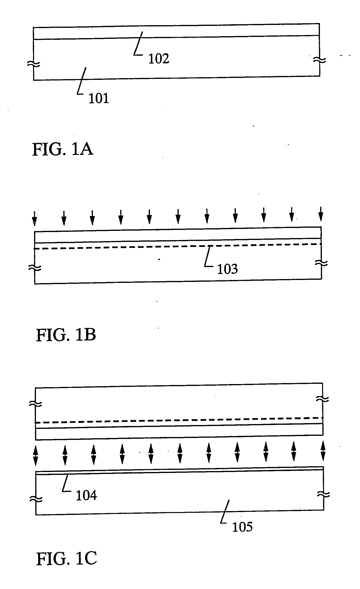
[0032] A structure of the present invention will be described with reference to FIGS. 1A to 1C and FIGS. 2A to 2D. First, a single crystal silicon substrate 101 is prepared. Next, a thermal oxidation treatment is carried out to form a silicon oxide film 102 on a major surface (component formation surface) of the substrate. Although the film thickness may be suitably determined by an operator, it is appropriate that the thickness is made 0.05 to 0.5 μm. This silicon oxide film 102 subsequently functions as a buried oxide film of an SOI substrate (FIG. 1A).
[0033] Next, hydrogen is added from the major surface side of the single crystal silicon substrate 101 through the silicon oxide film 102. In this case, it is appropriate that an addition of hydrogen is carried out by ion implantation method in the form of hydrogen ions. Of course, the adding step of hydrogen can be carried out by other means. In this way, a hydrogen added layer 103 is formed. In this embodiment, the hydrogen ion w...
embodiment 2
[0048] This embodiment is an example in which the sequence of the manufacturing steps of embodiment 1 is changed. Until the middle of the steps, steps are the same as in embodiment 1, so that their explanation will be omitted.
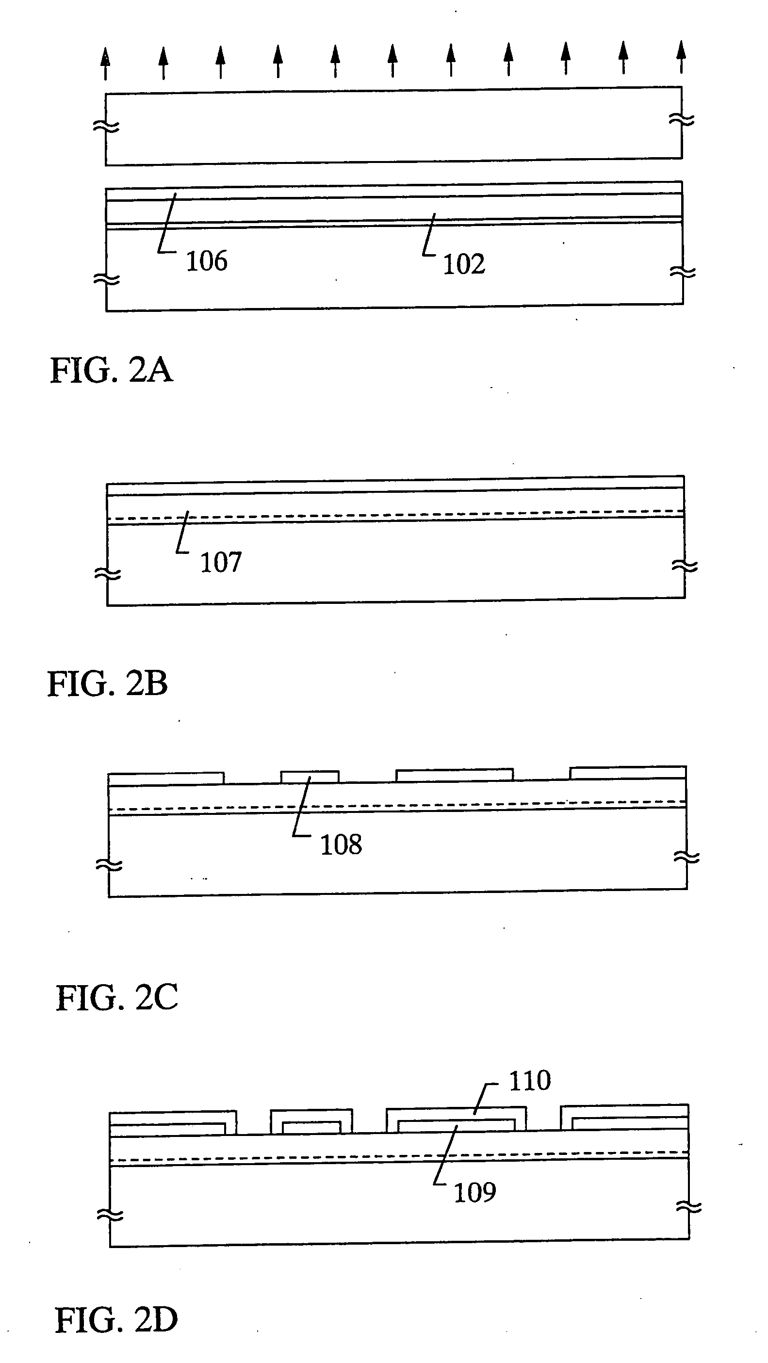
[0049] First, in the same procedure as in embodiment 1, steps until the substrate separating step of FIG. 2A are completed. Next, after the single crystal silicon thin film remaining on the second substrate is polished by means of such as CMP and is flattened, a patterning step is carried out to form island-like silicon layers.
[0050] When the island-like silicon layers are formed, a thermal oxidation treatment is carried out in that state. That is, the feature of this embodiment resides in that the stabilization of the bonded interface and the reduction of trap levels and defects in the island-like silicon layers are carried out by the same heat treatment (temperature range is 1050 to 1150° C.) simultaneously.
[0051] As described above, the second heat treatm...
embodiment 3
[0052] Embodiments 1 and 2 show examples in which trap levels and defects are reduced from the single crystal silicon thin films formed by Smart-Cut method. However, the present invention is also effective for a single crystal silicon thin film formed by other bonding SOI techniques.
[0053] In this embodiment, an example in which the present invention is applied to a single crystal silicon thin film formed by ELTRAN method as one of the bonding SOI techniques will be described with reference to FIGS. 3A to 3D and FIGS. 4A to 4D.
[0054] First, a single crystal silicon substrate 301 is prepared, and its major surface is subjected to anodic oxidation so that a porous silicon layer 302 is formed. It is appropriate that the anodic oxidation step is carried out in a mixture solution of hydrofluoric acid and ethanol. Since ELTRAN method itself is well known, the detailed description will be omitted here.
[0055] A single crystal silicon thin film 303 having a thickness of 100 nm is formed o...
PUM
| Property | Measurement | Unit |
|---|---|---|
| thickness | aaaaa | aaaaa |
| temperature | aaaaa | aaaaa |
| thickness | aaaaa | aaaaa |
Abstract
Description
Claims
Application Information