Method for fabricating semiconductor device

a memory device and semiconductor technology, applied in the field of memory device fabrication, can solve the problems of degrading device reliability and inefficient gate controllability, and achieve the effects of improving twr (write recovery time) and ltras (long time for row address strobe) characteristics, and decreasing the concentration of ion implanting a channel region

Inactive Publication Date: 2007-07-26
SK HYNIX INC
View PDF2 Cites 26 Cited by
  • Summary
  • Abstract
  • Description
  • Claims
  • Application Information

AI Technical Summary

Benefits of technology

[0011] According to the present invention, techniques for a method for fabricating a memory device are provided. In particular, the present invention provides a method for fabricating a semiconductor device wherein an epitaxial layer is formed over a device isolation structure of a recess gate region to form a semiconductor device including a SOI (Silicon-on-Insulator) channel structure, thereby decreasing ion implanting concentration of a channel region and improving tWR (Write Recovery time) and LTRAS (Long Time for Row Address Strobe) characteristics of the device.

Problems solved by technology

However, according to the above method for fabricating a semiconductor device, the gate is inefficient with respect to channel controllability.
Moreover, reliability of the device is degraded due to a body effect as bias voltage level of the device varies.

Method used


Image

  • Method for fabricating semiconductor device
  • Method for fabricating semiconductor device
  • Method for fabricating semiconductor device

Examples


Embodiment Construction

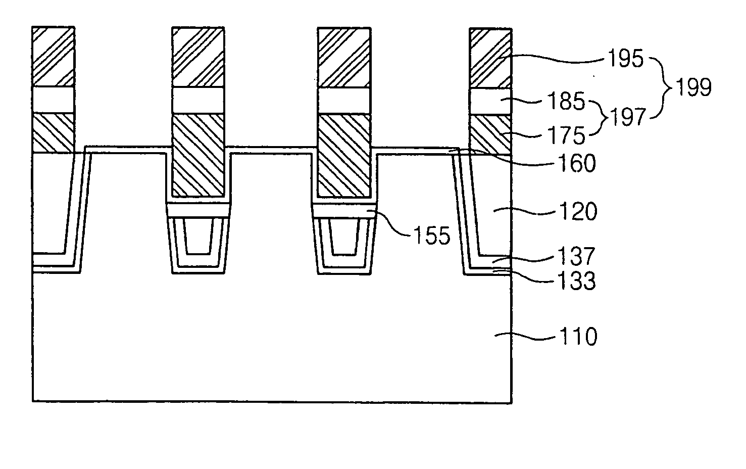
[0017] Reference will now be made in detail to exemplary embodiments of the present invention. Wherever possible, the same reference numbers will be used throughout the drawings to refer to the same or like parts. It should be appreciated that the embodiments are provided to describe and enable the invention to those skilled in the art. Accordingly, the embodiments described herein may be modified without departing from the scope of the present invention.

[0018]FIG. 3 is a simplified layout of a semiconductor device according to an embodiment of the present invention, wherein reference numerals 101, 103, and 105 denote an active region defined by the device isolation structure 120, a recess gate region, and a gate region, respectively.

[0019] Referring to FIG. 3, the active region 101 is disposed at the semiconductor substrate of a bit line contact region 107 and a storage node contact region 109. The recess region (or opening) 103 is a region extending from the bit line contact reg...


PUM


Abstract

A method for manufacturing a semiconductor device in accordance with an embodiment of the present invention provides a channel region formed over a device isolation structure to form a semiconductor device including a SOI (Silicon-on-Insulator) channel structure, thereby decreasing ion implanting concentration of a channel region and improving tWR (Write Recovery time) and LTRAS (Long Time for Row Address Strobe) characteristics of the device.

Description

BACKGROUND OF THE INVENTION [0001] The present invention relates to a method for fabricating a memory device. In particular, the present invention relates to a method for fabricating a semiconductor device wherein an epitaxial layer is formed over a device isolation structure of a recess gate region to form a semiconductor device including a SOI (Silicon-on-Insulator) channel structure, thereby decreasing ion implanting concentration of a channel region and improving tWR (Write Recovery time) and LTRAS (Long Time for Row Address Strobe) characteristics of the device. [0002]FIG. 1 is a simplified layout of a conventional semiconductor device, wherein reference numerals 1, 3, and 5 denote an active region, a recess gate region, and a gate region, respectively. [0003]FIGS. 2a through 2f are simplified cross-sectional views illustrating one method for fabricating a semiconductor device, wherein the cross-sectional views are taken along the line I-I′ of FIG. 1. [0004] Referring to FIG. 2...

Claims


Application Information

Patent Timeline
Patent Type & Authority Applications(United States)
IPC IPC(8): H01L21/8234
CPCH01L21/84H01L27/105H01L29/66613H01L27/1052H01L29/78636H01L29/78654H01L29/66772H10B99/00A47J45/061A47J45/062A47J36/34
Inventor LEE, EUN SUNG
Owner SK HYNIX INC
Why Eureka
Try Eureka