Method for fabricating bipolar integrated circuits

a technology of integrated circuits and fabrication methods, applied in the direction of resistors, diodes, semiconductor devices, etc., can solve the problems of unavoidable alignment errors, wafer area has not reached its best utilization rate, ic integration level has not reached its maximum, etc., to promote the integration level of integrated circuits, eliminate alignment errors resulting from multiple alignment operations of conventional technology, and accurately control the fabrication process

Inactive Publication Date: 2007-07-26
BCD SEMICON MFG
View PDF3 Cites 2 Cited by
  • Summary
  • Abstract
  • Description
  • Claims
  • Application Information

AI Technical Summary

Benefits of technology

[0008] The primary objective of the present invention is to provide a method for fabricating bipolar integrated circuits, which can promote the integration level of integrated circuits, wherein an LOCOS (Local Oxidation) technology is used to define all the element regions, which are to be formed in the active regions, such as N+ sinkers, isolations, extrinsic bases, bases, implant resistors, emitters and capacitors, in ord

Problems solved by technology

However, the other elements, such as resistors and capacitors, still need their own photomasks to fabricate, and there are still unavoidable alignment er

Method used


Image

  • Method for fabricating bipolar integrated circuits
  • Method for fabricating bipolar integrated circuits
  • Method for fabricating bipolar integrated circuits

Examples


Embodiment Construction

[0017] The present invention is to be described below in detail in cooperation with the drawings.

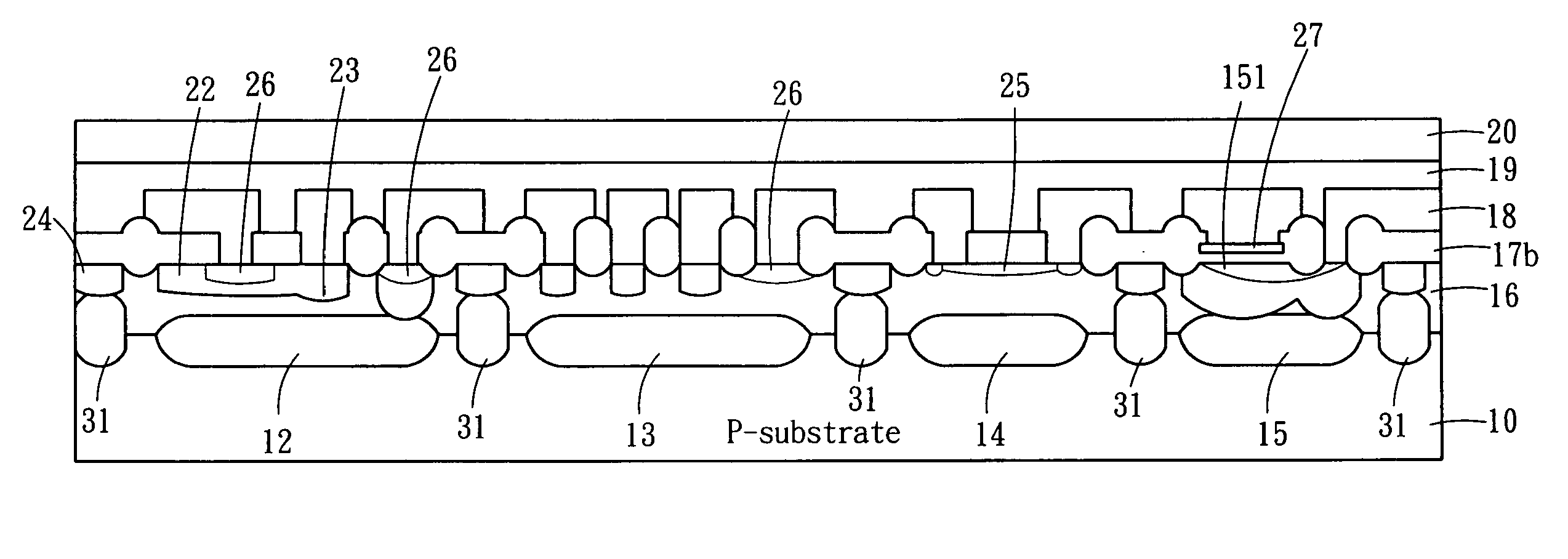
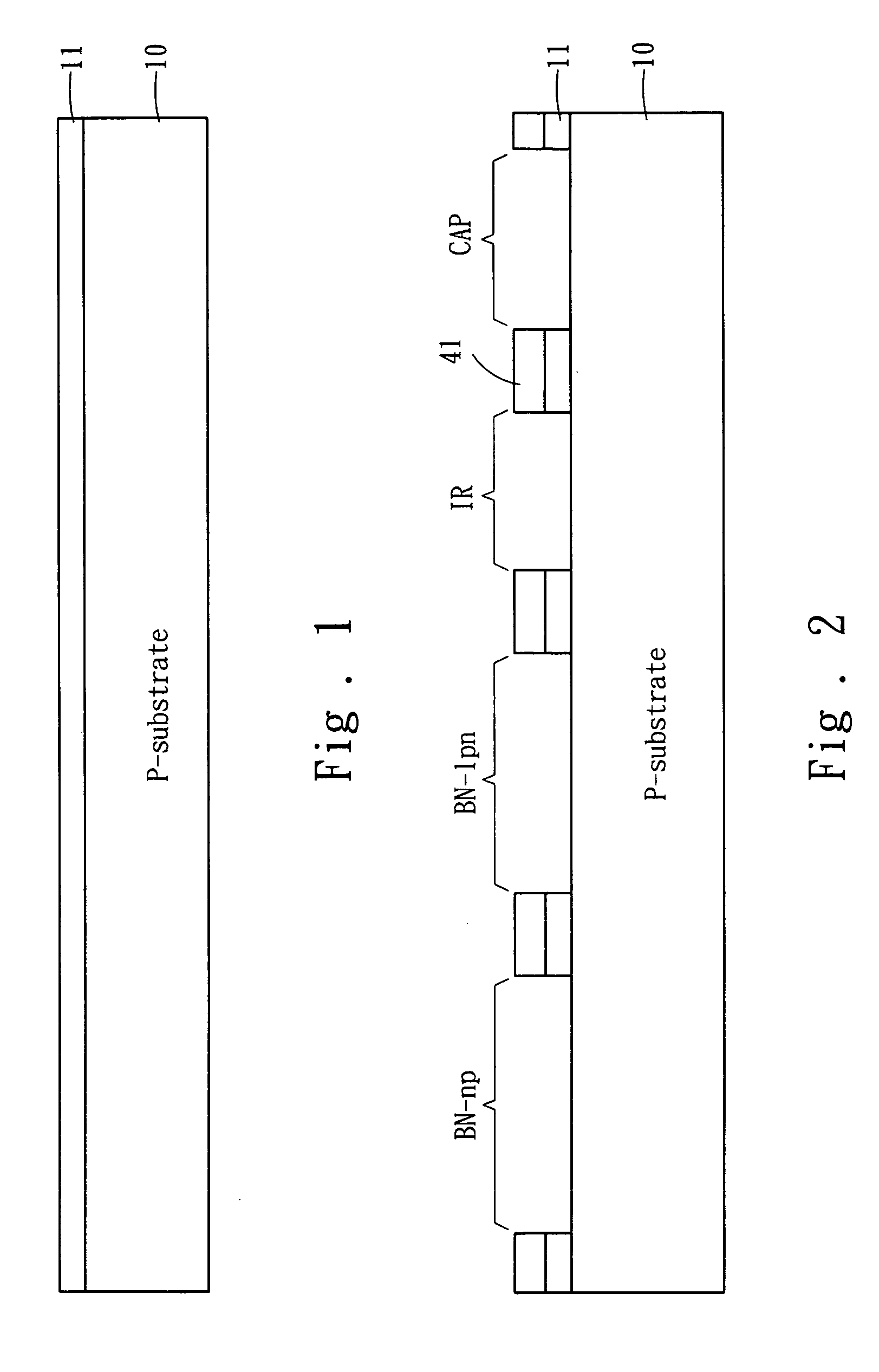
[0018] Refer to from FIG. 1 to FIG. 28 diagrams schematically showing the cross sections of the integrated circuit fabricated according to the method of the present invention. As shown in FIG. 1, a P-type substrate 10 is provided firstly, and an initial oxide layer 11 is formed on the surface of the P-type substrate 10. Next, as shown in FIG. 2, via a photolithographic process and a photoresist layer 41, the oxide layer 11 is etched to form BN-np, BN-lnp, IR (Implant Resistor), and CAP (Capacitor) regions of an N-type buried layer, which is needed in the succeeding procedures.

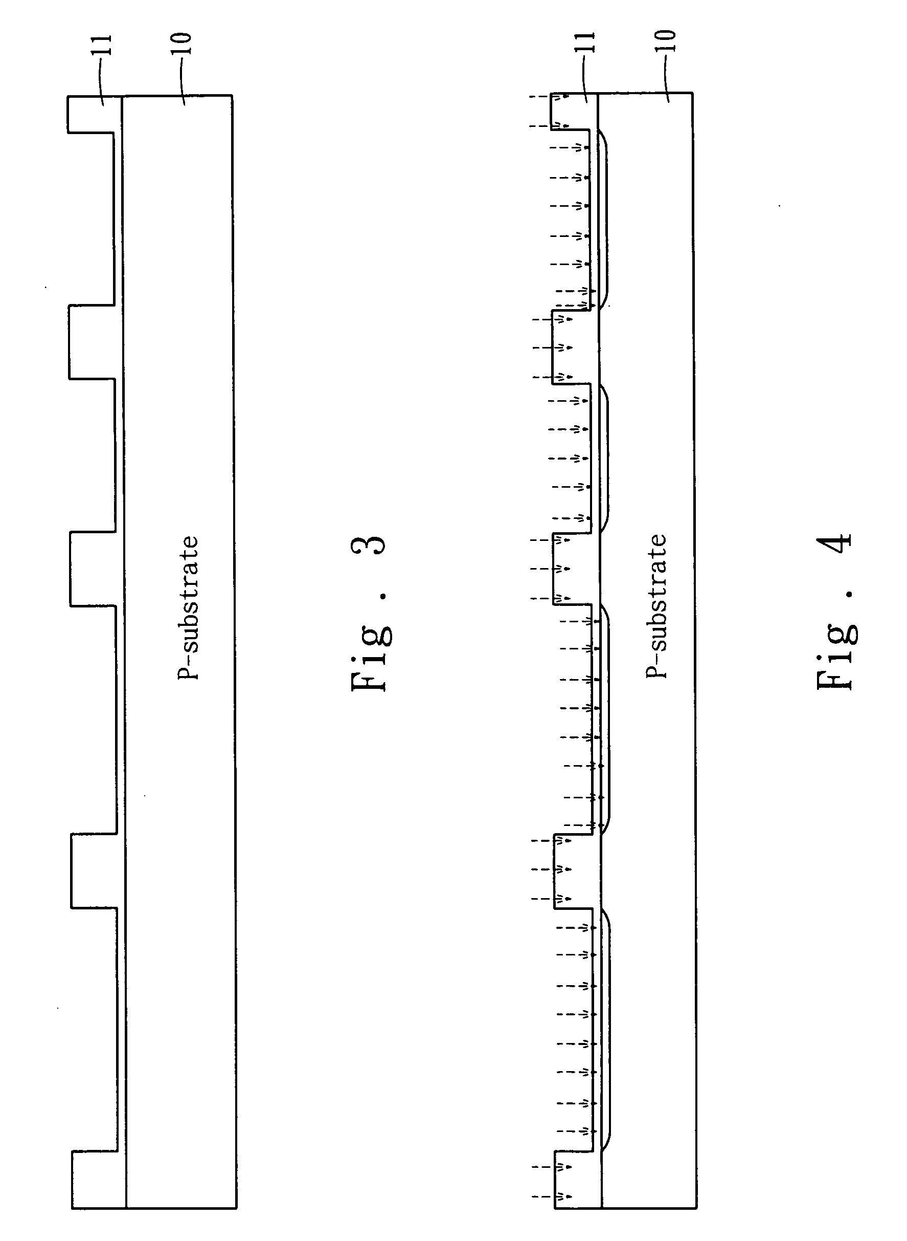
[0019] Next, as shown in FIG. 3, the P-type substrate 10 is pre-oxidized with a thermal oxidation process. Then, as shown in FIG. 4, N-type ions, such as Sb+ ions, are implanted into the BN-np, BN-lnp, IR, and CAP regions. Next, as shown in FIG. 5, a drive-in process is used to form an N-type NPN-transistor buried...


PUM


Abstract

The present invention discloses a method for fabricating bipolar integrated circuits, wherein LOCOS technology is used to define the active regions needed by all elements so that the self-alignment of the associated layers can be realized, and implant resistor regions are also directly defined in the active regions by local oxide layers; after base regions have been driven in the wafer, the resistors are implanted into the wafer so that the cost of resistor photomasks can be saved; silicon nitride is adopted to be the material of the dielectric layers of the capacitors, and with the characteristic of a buffering oxide etchant that etches oxide faster than it etches silicon nitride, the conventional deposition sequence of the dielectric layer is changed so that the formation of the dielectric layer needs only a single photomask.

Description

FIELD OF THE INVENTION [0001] The present invention relates to a method for fabricating integrated circuits, particularly to a method for fabricating bipolar integrated circuits, which can realize self-alignment and promote the integration level of circuits. BACKGROUND OF THE INVENTION [0002] For the semiconductor industry, the fabrication cost is closely related to the area of the epitaxial layer used in IC fabrication. Therefore, increasing IC integration level and decreasing the use of the epitaxial layer is the target of IC industry. [0003] The conventional method for fabricating bipolar IC comprises the following steps: providing a P-type substrate; forming an N-type buried layer; forming an N-type epitaxial layer; forming deep N+ sinkers; forming isolation buried regions; forming base regions; forming emitter regions; forming a contact metal; and forming a protection layer. [0004] To decrease the area occupied by isolations, a P-type buried layer may be formed in the P-type su...

Claims


Application Information

Patent Timeline
IPC IPC(8): H01L21/331H01L21/8222
CPCH01L21/8224H01L27/0658H01L28/20H01L27/0682H01L27/0821H01L27/067
Inventor ZENG, JINCHUANREN, CHONGQIU, BINLIU, XIAN-FENG
Owner BCD SEMICON MFG
Why Eureka
Try Eureka