High-density integration device and method for multi-source sensor

A technology of integrated devices and source sensors, applied in the direction of measuring devices, microstructure devices, processing microstructure devices, etc., can solve the problems of low power consumption and small volume, so as to improve utilization rate, improve production efficiency, and simplify the process of manufacturing Effect

Inactive Publication Date: 2018-07-17
INFORMATION SCI RES INST OF CETC
View PDF1 Cites 3 Cited by
  • Summary
  • Abstract
  • Description
  • Claims
  • Application Information

AI Technical Summary

Problems solved by technology

[0005] The invention discloses a multi-source sensor high-density integration device and method to solve the problems of high-precision, low power consumption, small volume, and light weight navigation requirements of existing micro-miniature platforms. The invention proposes a silicon-based The multi-functional substrate hybrid integration architecture of the adapter board rationally layered and assembled polarized light sensors, image sensors, inertial sensors, chip atomic clocks and other sensing and timing functional units, as well as power circuits, multi-source navigation solution circuits, and passive devices. On the silicon-based adapter board, at the same time, through TSV-RDL and metal ball bonding technology, the electrical signal connection between different functional board levels is realized. Through the 2.5-dimensional high-density assembly technology, the three-dimensional high-precision assembly of multiple substrates is realized, and finally multi-substrates are realized. High Density System Heterogeneous Integration of Various Sensing Units

Method used


Image

  • High-density integration device and method for multi-source sensor
  • High-density integration device and method for multi-source sensor

Examples


Embodiment 1

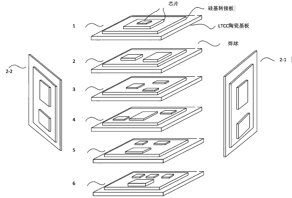
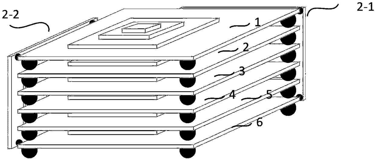
[0025] figure 1 It is an exploded view of a multi-source sensor high-density integrated device. The device is composed of six horizontal layers and two vertical function realization layers. The order of the six horizontal layers from top to bottom is polarization navigation realization layer 1 and X direction Inertial navigation layer 2-1, multi-source navigation fusion processing layer 3, energy supply layer 4, signal processing layer 5, image navigation and timing layer 6, the two vertical function realization layers are vertically arranged on the two sides of the six horizontal layers On the other hand, the two vertical function realization layers are respectively the Y-direction inertial navigation layer 2-2 and the Z-direction inertial navigation layer 2-3.

[0026] The horizontal layer is composed of a horizontal substrate and chips connected to the substrate, and the vertical function realization layer is composed of a vertical substrate and chips connected to the subst...

Embodiment 2

[0039] An integration method for a high-density integrated device of multi-source sensors, the device is composed of six horizontal layers and two vertical function realization layers, and the order of the six horizontal layers from top to bottom is polarization navigation realization layer, X Directional inertial navigation layer, multi-source navigation fusion processing layer, energy supply layer, signal processing layer, image navigation and timing layer, the two vertical function realization layers are set on both sides of the six horizontal layers, and the two vertical The function realization layers are the inertial navigation layer in the Y direction and the inertial navigation layer in the Z direction. Each horizontal layer of the device includes a horizontal substrate and a chip. On the silicon-based interposer, the chips are heterogeneously integrated on the silicon-based interposer in a 2.5-dimensional heterogeneous integration manner.

[0040] The integration sequ...


PUM


Abstract

The invention discloses a high-density integration device for a multi-source sensor. The device is composed of six horizontal layers and two vertical function realization layers; the six horizontal layers comprise a polarization navigation realization layer, an X-direction inertia navigation layer, a multi-source navigation fusion processing layer, an energy supply layer, a signal processing layerand an image navigation and timing layer from top to bottom in sequence; the two vertical function realization layers are vertically arranged on two sides of the six horizontal layers; and the two vertical function realization layers comprise a Y-direction inertia navigation layer and an X-direction inertia navigation layer respectively. The device has the beneficial effects that a multifunctional substrate hybrid integrated framework based on a silicon substrate adapter plate is adopted, electrical signal interconnection among substrates is realized by adopting TSV silicon through holes, RDLre-wiring and metal ball bonding technology, and high-density 2.5-dimensional stacking and integration of a navigation sensing system chip-level module based on different principles is facilitated, so that the volume and weight of a micro system are greatly reduced, the utilization rate of the system space is improved, and the integration level is improved.

Description

technical field [0001] The invention relates to the field of heterogeneous integrated manufacturing of microsystems, in particular to a high-density integrated device and method for multi-source sensors. Background technique [0002] The navigation system is a necessary means for mobile platforms such as vehicles, aircrafts, and ships to obtain real-time position and direction and complete the scheduled tasks on time. Based on different principles, various navigation methods such as satellite, inertial, geomagnetic, astronomical, and images have emerged. However, single-source navigation is often limited by specific environments or conditions, and it is difficult to meet the navigation requirements in long-term, unknown, and complex environments. [0003] Combined navigation, which organically combines two or more navigation methods, has gradually evolved into the main mode of modern navigation. The integrated navigation system can give full play to the advantages of each ...

Claims


Application Information

Patent Timeline
Patent Type & Authority Applications(China)
IPC IPC(8): G01C21/16B81B7/00B81B7/02B81C3/00
CPCB81B7/0006B81B7/0074B81B7/02B81C3/001G01C21/16
Inventor 王刚汪志强吕小微
Owner INFORMATION SCI RES INST OF CETC
Why Eureka
Try Eureka