Method of manufacturing field emission device

Inactive Publication Date: 2007-08-02
SAMSUNG SDI CO LTD
View PDF10 Cites 13 Cited by
  • Summary
  • Abstract
  • Description
  • Claims
  • Application Information

AI Technical Summary

Benefits of technology

[0008]The present invention provides a method of manufacturing a field emission device (FED) that has a small number of photomask pa

Problems solved by technology

In a FED, a silicon tip or a molybdenum tip has been used as an emitter tip, but since silicon and molybdenum tips have short lifetimes and low stability, the electron emission efficiency thereof is low.
However, when emitter holes are manufactured in a plurality of photolithography proces

Method used


Image

  • Method of manufacturing field emission device
  • Method of manufacturing field emission device
  • Method of manufacturing field emission device

Examples


Example

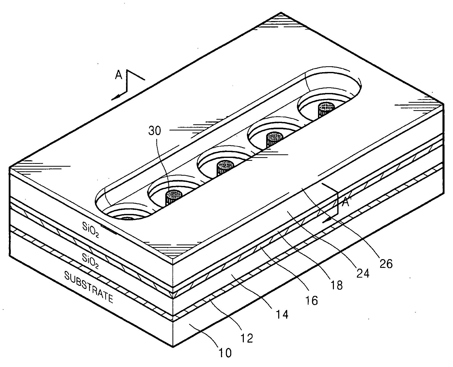
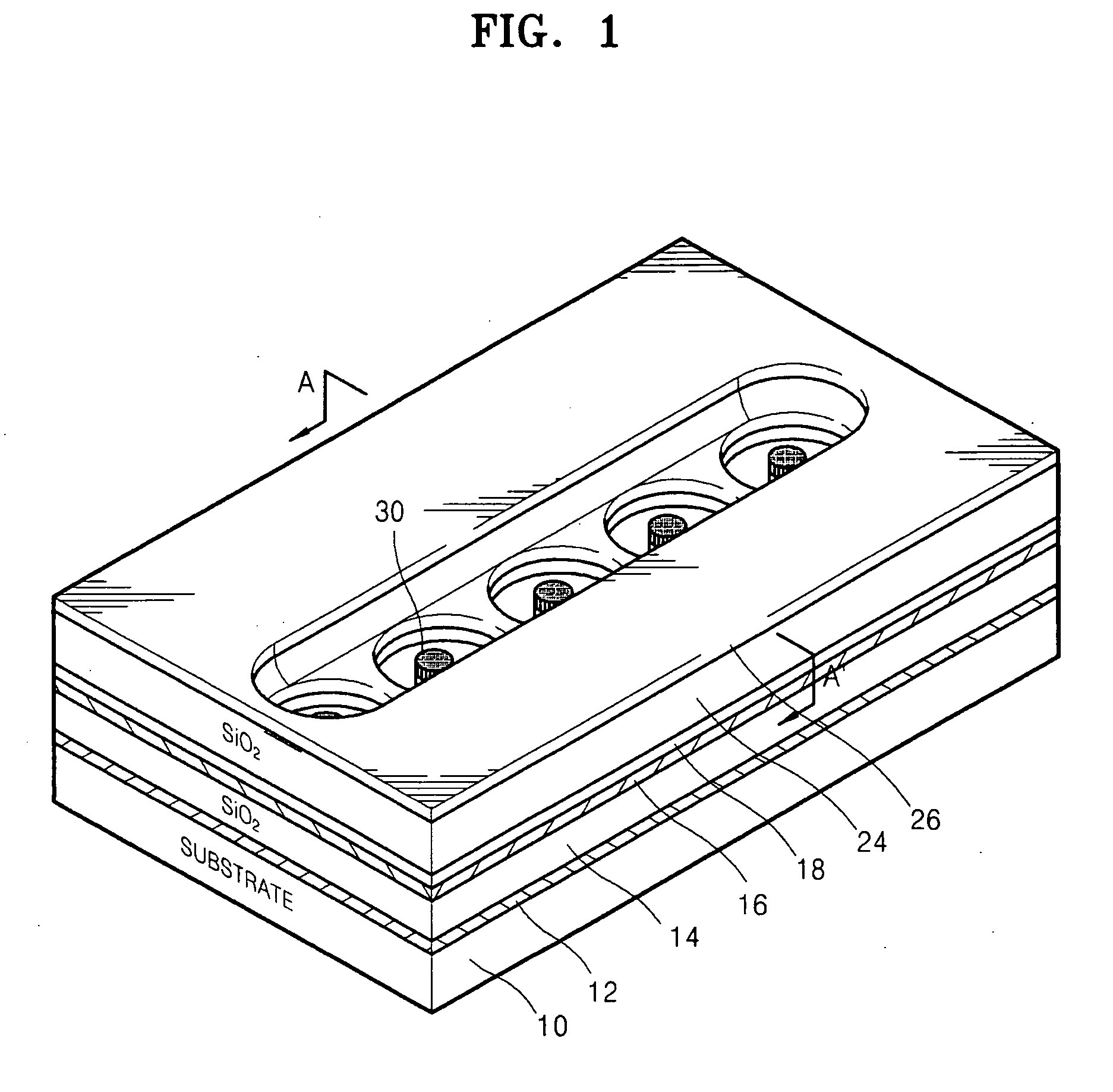
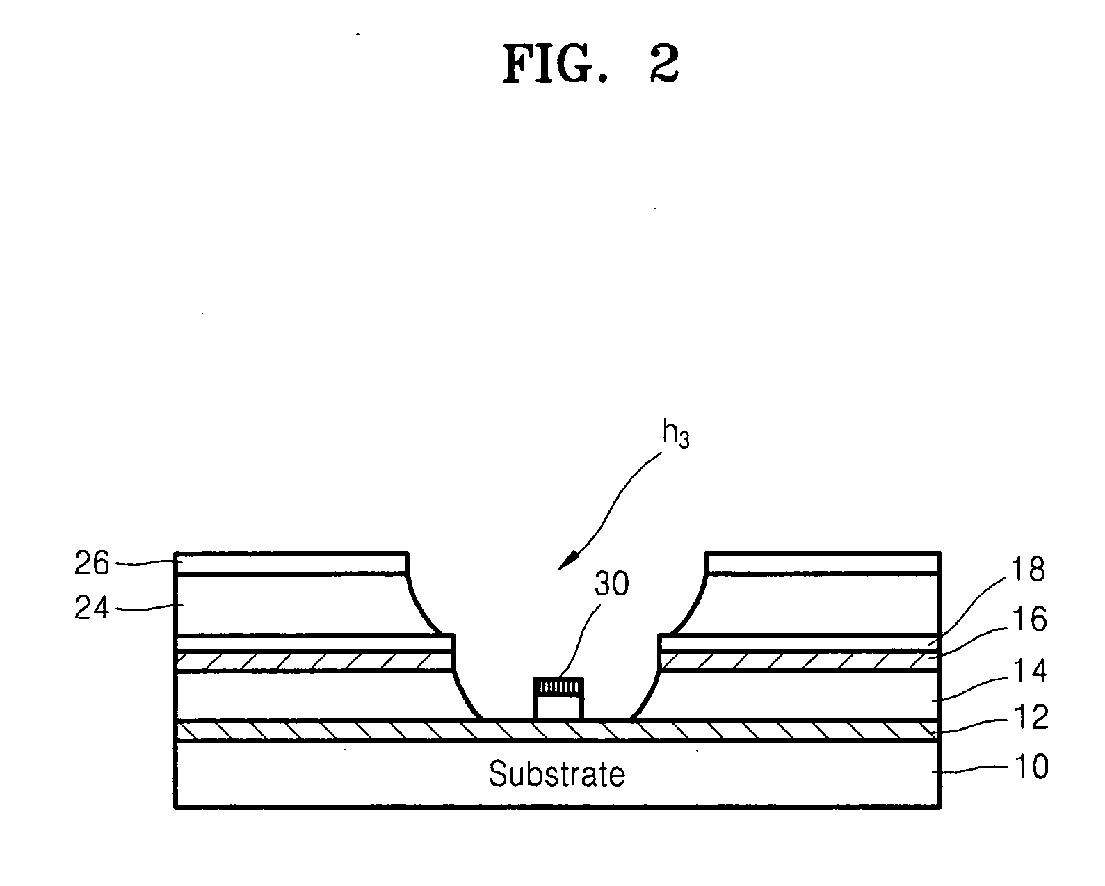
[0020]The present invention will now be described more completely with reference to the accompanying drawings, in which exemplary embodiments of the invention are shown. In the drawings, the thicknesses of layers and regions are exaggerated for clarity.

[0021]FIG. 1 is a perspective view of a field emission device (FED) manufactured as an embodiment of the present invention. FIG. 2 is a cross-sectional view of the FED of FIG. 1 cut along a line A-A′. Referring to FIGS. 1 and 2, a plurality of emitter holes h3 are arranged in a row, and electron emission emitter 30 is formed in each of emitter holes h3. Electron emission emitters 30 may be made of a carbon nanotube material.

[0022]Cathode layer 12 is interposed between electron emission emitters 30 and substrate 10. First insulating layer 14, gate layer 16, protection layer 18, second insulating layer 24, and focus electrode layer 26 are sequentially formed on cathode layer 12, and have holes on their layers to expose electron emission...


PUM


Abstract

A method of manufacturing a field emission device (FED), which reduces the number of photomask patterning processes and improves the manufacturing yield of the FED, is provided. The method includes steps of sequentially forming a cathode layer, a first insulating layer, and a gate layer on a substrate, forming a protection layer on the gate electrode layer, etching portions of the protection layer and gate electrode to form a plurality of first opening holes where portions of the first insulating layer being exposed through the first opening holes, forming a second insulating layer on the protection layer and on the first opening holes, forming a focus electrode layer on the second insulating layer, forming a photoresist layer on the focus electrode layer, etching a portion of the photoresist layer and a portion of the focus electrode layer to form a second opening hole where a portion of the second insulating layer being exposed through the second opening hole, and forming emitter holes exposing a portion of the cathode layer by etching the exposed surface of the second insulating layer to a bottom surface of the first insulating layer. After removing the photoresist layer electron emission emitters are formed on the cathode layer.

Description

CLAIM OF PRIORITY[0001]This application makes reference to, incorporates the same herein, and claims all benefits accruing under 35 U.S.C.§119 from an application for METHOD OF MANUFACTURING FIELD EMISSION DEVICE earlier filed in the Korean Intellectual Property Office on 2 Feb. 2006 and there duly assigned Serial No. 10-2006-0010057.BACKGROUND OF THE INVENTION[0002]1. Field of the Invention[0003]The present invention relates to a field emission device (FED), and more particularly, to a method of manufacturing an FED in which the number of photomask patterning processes is small and an emitter hole forming process can be precisely controlled to improve the manufacturing yield of the FED.[0004]2. Description of the Related Art[0005]A field emission device (FED) is a color image display that realizes a color image by applying an electric field to an emitter formed on an electrode to emit an electron beam from the emitter onto a phosphor material.[0006]The core technology of a FED lies...

Claims


Application Information

Patent Timeline
IPC IPC(8): H01L31/00
CPCH01J9/025H01J3/021B26F1/32
Inventor CHOI, JUN-HEEKANG, HO-SUKBAIK, CHAN-WOOKKIM, HA-JONG
Owner SAMSUNG SDI CO LTD
Why Eureka
Try Eureka