Semiconductor device

a technology of semiconductor devices and heat dissipation design, which is applied in the direction of semiconductor devices, semiconductor/solid-state device details, electrical equipment, etc., can solve the problems of increasing the cost of products, and being unable to cope with miniaturization, so as to reduce the number of parts, reduce the number of mounting areas, and high intelligent functions

Inactive Publication Date: 2007-08-02
RENESAS TECH CORP
View PDF5 Cites 65 Cited by
  • Summary
  • Abstract
  • Description
  • Claims
  • Application Information

AI Technical Summary

Benefits of technology

[0018] To make highly intelligent functions and reduction in the mounting area compatible, reduction in the number of parts and stacked mount are required. However, there exists a problem that, when the stacked mount is carried on, the temperature of the part at a distant position seen from the circuit substrate of a mobile information terminal main body, that is, a so-called mother board, that is, the temperature of the part disposed on the surface far away from a surface having a connecting unit with the mother board is apt to rise. Further, in general, the cost of the semiconductor device is apt to rise when it is highly functionalized, and goes down when the mounting area becomes smaller, but the cost lowering pressure by the reduction in the mounting area is apt to be stronger than the cost rising pressure by high functionalization. Consequently, granted that the mounting area can be reduced or that a structure capable of inhibiting the temperature rise of the parts can be realized, there is a need to avoid the rise of the material cost of the product as much as possible by adding new parts for that reason.

Problems solved by technology

In the prior art disclosed in the Patent Document 1, a heat conducting member to function as a heat diffusion plate includes only an earth function that connects a semiconductor element rear surface and a wiring substrate in circuit-wise, and there is a problem that when signal wirings are provided by means such as wire bonding, a mounting area becomes large.
Further, addition of the heat diffusion plate invites an increase in the number of parts and connecting members as well as the mounting process thereof, thereby causing a problem of increasing the cost of products.
Furthermore, since it is presumed that a number of semiconductor elements are basically dispersed and mounted on a flat surface, there is a problem that the semiconductor device for mobile information terminal for which high functionalization and miniaturization are in great demands in the market is unable to cope with miniaturization due to an increase in the mounting area when the number of parts and functions per each element are increased.
On the other hand, in the prior art disclosed in the Patent Document 2, while the problem of miniaturization can be solved, there is a need to fit semiconductor elements that mainly generate heat into the wiring substrate, and this makes the manufacturing process complicated, and causes a problem of the cost of products becoming high.
However, in the case of the element such as a power amplifier(power amp) used for transmission and reception of the mobile phone, it is common that the elements dissipating heat at different time zone and place depending on the frequency bands and standards to be used are mixedly loaded in one. semiconductor device (module), and in order to miniaturize and highly functionalize the mixedly loaded mounting structure of the semiconductor device such as a power amp, which is large in heat value and generates heat at different timing, there has been a problem that the lead frame is not necessarily effective.

Method used


Image

  • Semiconductor device
  • Semiconductor device
  • Semiconductor device

Examples


first embodiment

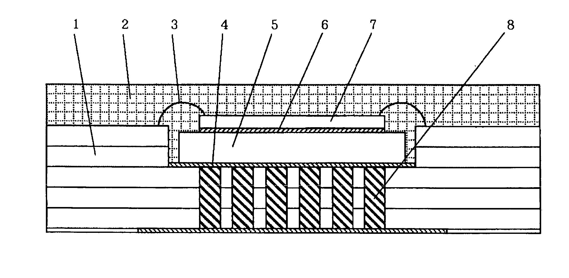
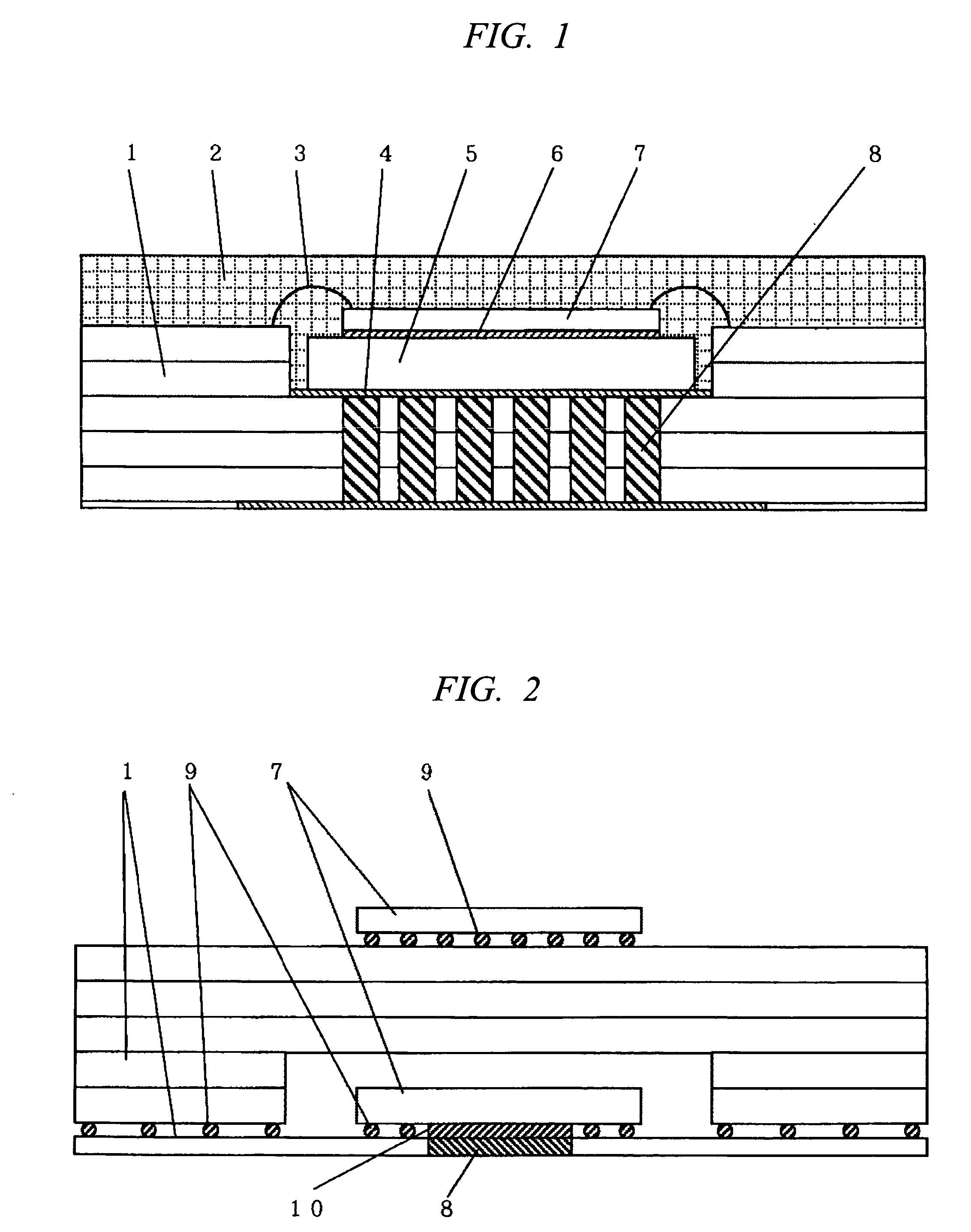
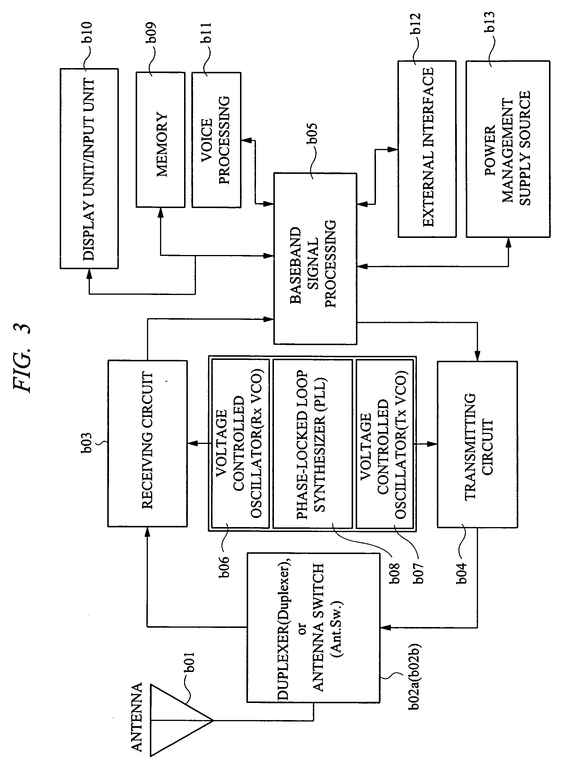
[0080] The embodiment of the present invention will be described with reference to FIGS. 4 to 11. FIG. 4 is a block system diagram showing the outline of a signal processing circuit mounted on a mobile information terminal in the present embodiment, and a semiconductor device in the present embodiment takes a power amp of FIG. 4 as a target. FIG. 5 is a sectional view showing a mounting structure of a power amplifier (power amp) in the present embodiment, FIG. 6 is a view showing one example of an element sectional structure of a bipolar transistor from among the power amplifiers in the present embodiment, FIG. 7 is a sectional view showing an example forming a combination heat dissipation and large area bump on an emitter wiring when the bipolar transistor of FIG. 6 is flip-chip mounted, and FIG. 8 is a view in the case where one example of signal pad electrode and an amplifier circuit seen from the element surface side of the bipolar transistor.

[0081] On the other hand, FIG. 9 is...

second embodiment

[0091] Another embodiment of the present invention will be described by using FIG. 12. The present embodiment is characterized in that a first semiconductor element 701 is flip-chip connected from among the mounting structures of the embodiment shown in FIGS. 4 to 11, and is mounted on a wiring substrate 1 by a first connecting bump 901, and upon thereof, a second semiconductor element 702 is laminated in a stacked state by a second connecting bump 902 and a combination heat dissipation and large area bump 10.

[0092] In the present embodiment shown in FIG. 12, though there is a problem that heat resistance is increased between the first semiconductor element 701 and a wiring substrate 1 by flip-chip connecting the first semiconductor element 701, a heat generating region of the element that generates heat at different time is within an overlapped range seen from a normal line of the wiring substrate 1, the effect of the first semiconductor element 701 functioning as a heat diffusion...

third embodiment

[0094] Another embodiment of the present invention will be described by using FIG. 13. The present embodiment is characterized by forming a through-hole electrode 13 in a first semiconductor element 701 from among the mounting structures of the embodiment shown in FIG. 12, and performing all the exchanges of signals between wiring substrate 1 and the first semiconductor element 701 and a second semiconductor element 702 through a first signal connecting bump 901, thereby making wire bonding unnecessary.

[0095] While the embodiments of the present invention shown in FIGS. 12 and 13 show a structure in which the first semiconductor elements 701 to be flip-chip connected are all connected to the wiring substrate 1 by the first signal connecting bump 901, if the bump 901 is uniform in height at the product mounting time so that the first semiconductor element 701 and the wiring substrate 1 are surely connected, there is no problem even if the area thereof is different. of course, it doe...


PUM


Abstract

Heating elements different in heat generating timing are laminated in a stacked state, and the heating element close to a wiring substrate is allowed to function as a heat diffusion plate for another heating element.

Description

CROSS-REFERENCE TO RELATED APPLICATION [0001] The present application claims priority from Japanese Patent Application No. JP 2006-003195 filed on Jan. 11, 2006, the content of which is hereby incorporated by reference into this application. TECHNICAL FIELD OF THE INVENTION [0002] The present invention relates to a heat dissipation design technique for a radio frequency transmitting and receiving semiconductor device mounted on a mobile information terminal such as a mobile phone. BACKGROUND OF THE INVENTION [0003] As a technique regarding a heat dissipation design for a radio frequency transmitting and receiving power semiconductor device mounted on a mobile information terminal such as a mobile phone, a mounting structure for reducing the heat resistance is disclosed, for example, in Japanese Patent Application Laid-Open Publication No. 2001-102483 (Patent Document 1) and Japanese Patent Application Laid-Open Publication No. 2004-71597 (Patent Document 2). From among these documen...

Claims


Application Information

Patent Timeline
Patent Type & Authority Applications(United States)
IPC IPC(8): H01L23/52H01L23/48
CPCH01L23/3121H01L23/34H01L2924/1305H01L2224/16235H01L2924/13091H01L2924/13064H01L2224/73203H01L2224/32145H01L2225/06568H01L2924/1515H01L2224/13025H01L2224/32225H01L2224/16225H01L24/73H01L24/48H01L2924/1815H01L2924/1517H01L2924/15153H01L2225/06589H01L2225/06582H01L2225/06541H01L23/3677H01L25/0657H01L2223/6644H01L2223/6688H01L2224/16145H01L2224/16237H01L2224/48091H01L2224/48227H01L2224/73265H01L2225/0651H01L2225/06513H01L2225/06517H01L2924/00014H01L2224/48237H01L2924/00H01L2924/00012H01L2924/181H01L2924/14H01L2224/73257H01L2224/45099H01L2224/45015H01L2924/207
Inventor OSONE, YASUOKAWANO, KENYAYORITA, CHIKOHASEGAWA, YUSHIRAI, YUJITANAKA, NAOTAKATOMOI, SEIICHIOKABE, HIROSHI
Owner RENESAS TECH CORP
Why Eureka
Try Eureka