Display device

Active Publication Date: 2007-08-02
SEMICON ENERGY LAB CO LTD
View PDF18 Cites 42 Cited by
  • Summary
  • Abstract
  • Description
  • Claims
  • Application Information

AI Technical Summary

Benefits of technology

[0017]A narrow frame of a display panel can be realized because a common wiring can be formed in the end portion of the substrate in substitution for a lead wiring over an active matrix substrate so that expansion of a frame portion over the substrate

Problems solved by technology

In addition, the active matrix display devices are small and lightweight, and consume low power.
However, in order to increase the width of the lead w

Method used


Image

  • Display device
  • Display device
  • Display device

Examples


embodiment mode 1

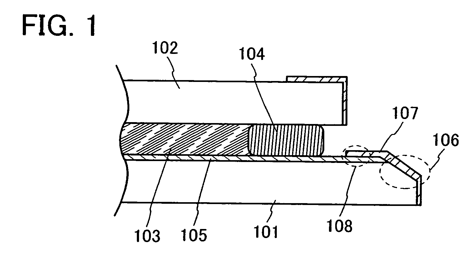
[0031]This embodiment mode will explain a liquid crystal panel used for a liquid crystal display device as an example of a display panel used for a display device. Specifically, a liquid crystal material is sandwiched between an active matrix substrate and an opposite substrate by a One Drop Filling (ODF) method. After attaching the both substrates, an element forming surface side of the end portion of the active matrix substrate is chamfered, a common wiring is formed in a chamfer portion or the like, and wirings (a source line, a gate line, a storage capacitor line, a leading out wiring, and the like) formed over the active matrix substrate are electrically connected by the common wiring. A case having such a structure will be explained. Note that the leading out wiring is an extracted portion of the source line, a gate line, the storage capacitor line, or the like, which is formed outside the pixel portion, and which connects the pixel portion and an external circuit.

[0032]FIG. 1...

embodiment mode 2

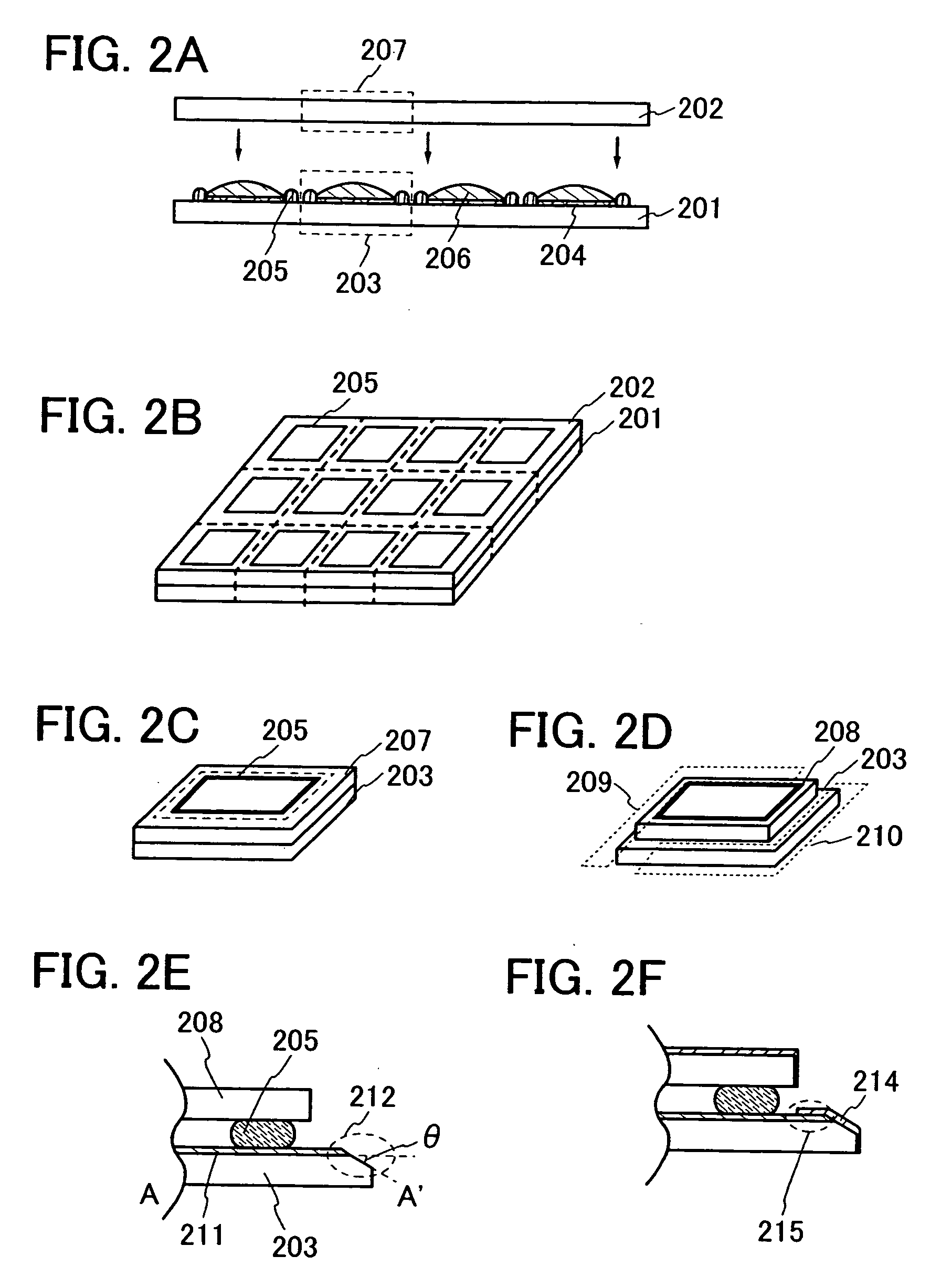
[0051]This embodiment mode will explain a liquid crystal panel used for a liquid crystal display device as an example of a display panel used for a display device. Specifically, after attaching an active matrix substrate, an element forming surface side of the end portion which is chamfered in advance, to an opposite substrate, a liquid crystal material is sandwiched between the both substrates, a common wiring is formed in a chamfer portion or the like, and wirings (a source line, a gate line, a storage capacitor line, a leading out wiring, and the like) formed over the active matrix substrate are electrically connected by the common wiring. A case having such a structure will be explained.

[0052]FIG. 4 shows a cross section of the end portion of a liquid crystal panel formed by being injected with a liquid crystal material 403 after attaching an active matrix substrate 401, which is chamfered in advance, and an opposite substrate 402 to each other with a sealant 404. Note that, alt...

embodiment mode 3

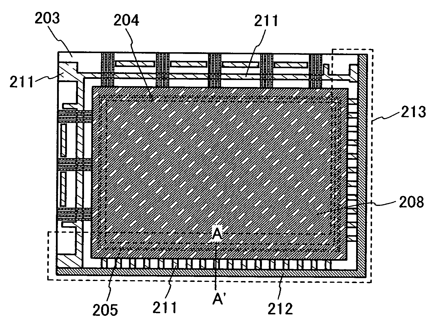
[0069]As the manufacturing method of the active matrix substrate that can be used for Embodiment Mode 1 or 2, this embodiment mode will particularly explain a manufacturing method of an amorphous silicon thin film transistor (TFT) and a pixel electrode formed in a pixel portion (reference numeral 204 of FIG. 3B and reference numeral 513 of FIGS. 6A and 6B) over an active matrix substrate, with reference to FIGS. 7A to 7E and FIGS. 8A to 8D. Note that explanation will be given in FIGS. 7A to 7E and FIGS. 8A to 8D with the common reference numerals.

[0070]As shown in FIG. 7A, a first conductive film 702 is formed over a substrate 701. The first conductive film 702 can be formed using a film formation method such as sputtering, PVD, CVD, droplet discharging, printing, or electroplating. As the material that is used to form the first conductive film 702, for example, a metal element such as Ag, Au, Cu, Ni, Pt, Pd, Ir, Rh, W, Al, Ta, Mo, Cd, Zn, Fe, Ti, Si, Ge, Zr, Ba, or Nd, an alloy mat...


PUM


Abstract

It is an object of the present invention to provide a display device where expansion of a frame portion over a substrate, which results from formation of a lead wiring over an active matrix substrate, is minimally suppressed to realize a narrow frame. According to one feature of a display device of the present invention, a chamfer portion is formed at least at an end portion of an active matrix substrate having a pixel portion of a pair of substrates disposed to be opposed to each other, and wirings (a source line, a gate line, a storage capacitor line, a leading out wiring, and the like) over the active matrix substrate are electrically connected by a common wiring formed in the chamfer portion.

Description

BACKGROUND OF THE INVENTION[0001]1. Field of the Invention[0002]The present invention relates to an active matrix display device having an active matrix display portion which is structure by formation of a thin film transistor (hereinafter, referred to as a TFT) over a substrate.[0003]2. Description of the Related Art[0004]Conventionally, display devices typified by a liquid crystal display device and a light-emitting device have been known as active matrix display devices using active elements such as TFTs. In these active matrix display devices, pixel density can be increased. In addition, the active matrix display devices are small and lightweight, and consume low power. Accordingly, products using active matrix display devices such as a monitor for a computer, a television, and a monitor for a car navigation system have been developed as one of flat panel displays in substitution for a CRT display.[0005]In addition, each of these active matrix display devices has a structure inc...

Claims


Application Information

Patent Timeline
IPC IPC(8): G02F1/1345
CPCG02F1/1345G02F1/134309G02F1/133308G02F2001/13456G02F1/13456G02F1/133305G02F1/13452G02F1/134363
Inventor HOSOYA, KUNIO
Owner SEMICON ENERGY LAB CO LTD
Why Eureka
Try Eureka