Display device

a display device and display technology, applied in thermoelectric devices, identification means, instruments, etc., can solve the problems of difficult realization of next-generation television sets, limited application, and bcp is, therefore, hardly usable, and achieve the effects of improving the efficiency of charge injection into each light-emitting unit, improving lifetime characteristics, and improving brightness

Active Publication Date: 2007-08-09
JOLED INC
View PDF5 Cites 57 Cited by
  • Summary
  • Abstract
  • Description
  • Claims
  • Application Information

AI Technical Summary

Benefits of technology

[0015] In the first and second, invention display devices, the efficiency of charge injection into each light-emitting unit has been improved owing to the use of such a material as an oxide, which includes at least one of alkali metals and alkaline earth metals, or a fluoride, which includes at least one of alkali metals and alkaline earth metals, in at least a portion of each charge generation layer as described above. As a consequence, it becomes possible to achieve an improvement in brightness and improvements in lifetime characteristics, in other words, improvements in long-term reliability owing to improvements in environmental stability in a stacked display device having light-emitting units composed of organic layers, respectively, and stacked together. Further, the above-mentioned material such as the oxide, which includes at least one of alkali metals and alkaline earth metals, or the fluoride, which includes at least one of alkali metals and alkaline earth metals, is used in the form of the oxide or fluoride from the stage of the film formation, and therefore, is stable so that each charge generation layer making use of the material is also stable. Furthermore, such charge generation layers excellent in the characteristics of charge injection are formed with the stable material, and therefore, it is no longer required to conduct the formation or the like of their films while taking into consideration the stoichiometric ratio in the fabrication of the device, thereby facilitating the fabrication.
[0016] In the third invention display device, the stacked display device has been improved in the efficiency of light emission owing to the use of the charge generation layer made of stable materials such as an organic compound and an alkali metal and / or alkaline earth metal. As a consequence, in a stacked display device having light-emitting units composed of organic layers, respectively, and stacked together, it becomes possible to achieve an improvement in brightness and improvements in lifetime characteristics, in other words, improvements in long-term reliability owing to improvements in environmental stability as in the first and second display devices. Furthermore, such charge generation layers excellent in the characteristics of charge injection are formed with the stable material, and therefore, it is no longer required to conduct the formation or the like of their films while taking into consideration the stoichiometric ratio in the fabrication of the device, thereby facilitating the fabrication.

Problems solved by technology

However, the lowering of the initial brightness results in a limitation to the application in its practical use, negates by itself the potential of the organic electroluminescent device, and hence, makes it difficult to realize a next-generation television set.
Therefore, the stoichiometric ratio of the individual materials that makes up the electron injection layer 7 is important, and its imbalance is considered to result in unstableness even as a layer.
BCP is, therefore, hardly usable when the stability of a device is taken into consideration.
In addition, another problem is considered to exist in that a device making use of BCP has poor reliability in environmental stability.

Method used


Image

  • Display device
  • Display device
  • Display device

Examples


first embodiment

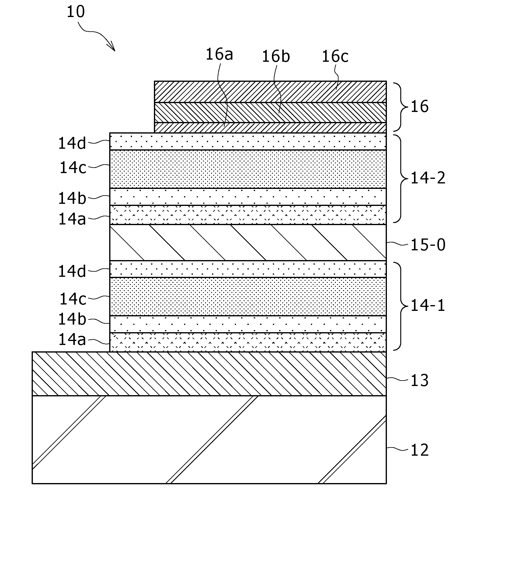
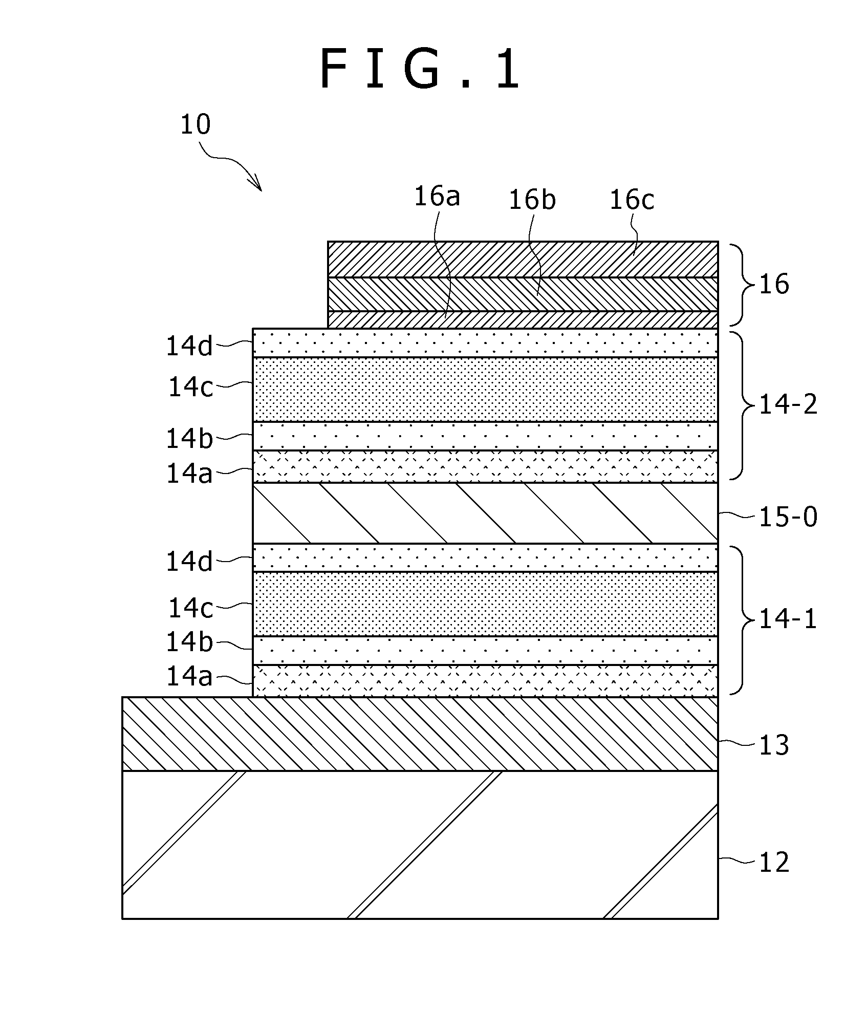
[0034]FIG. 1 is a cross-sectional view showing one construction example of a display device according to the first embodiment. The display device 10 shown in this drawing is a stacked display device 10 composed of light-emitting units stacked one over the other, and is provided with an anode 13 arranged on a substrate 12, plural light-emitting units 14-1,14-2, . . . (two in this embodiment) stacked together and arranged on the substrate 13, a charge generation layer 15-0 arranged between these light-emitting units 14-1,14-2, and a cathode 16 arranged as a top layer on the light-emitting unit 14-2.

[0035] A description will hereinafter be made of the construction of a surface-emitting display device that light produced upon recombination of holes, which have been injected from the anode 13, and electrons, which have been generated in the charge generation layer 15-0, within the light-emitting unit 14-1 and light produced upon recombination of electrons, which have been injected concu...

second embodiment

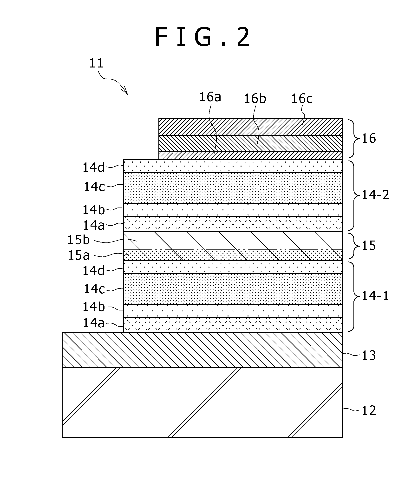
[0066]FIG. 2 is a cross-sectional view showing one construction example of a display device according to the second embodiment. A display device 11 shown in this drawing is different in the construction of a charge generation layer 15 from the display device 10 described with reference to FIG. 1, and in the remaining construction, they are supposed to be similar to each other. Centering around the charge generation layer 15, the construction of the display device 11 according to the second embodiment will hereinafter be described in detail.

[0067] Specifically, in the display device 11 according to the second embodiment, the charge generation layer 15 arranged between the light-emitting unit 14-1 and the light-emitting unit 14-2 has been formed using an oxide which contains at least one (at least one element) of alkali metals and alkaline earth metals. This charge generation layer 15 has a construction that an interfacial layer 15a and an intrinsic charge generation layer 15b are st...

third embodiment

[0087]FIG. 3 is a cross-sectional view showing one construction example of a display device according to the third embodiment. A display device 11′ shown in this drawing is different in the construction of a charge generation layer 15′ from the display device 10 described with reference to FIG. 1, and in the remaining construction, they are supposed to be similar to each other. Centering around the charge generation layer 15′, the construction of the display device 11′ according to the third embodiment will hereinafter be described in detail.

[0088] Specifically, the charge generation layer 15′ in the display device 11′ according to the third embodiment has a construction that an interfacial layer 15a′ and an intrinsic charge generation layer 15b are stacked together in this order from the side of the anode 13. Because this interfacial layer 15a′ acts as a cathode for the light-emitting unit 14-1 arranged in contact with the anode 13 as in the second embodiment, this interfacial lay...


PUM

PropertyMeasurementUnit
thicknessaaaaaaaaaa
thicknessaaaaaaaaaa
thicknessaaaaaaaaaa

Abstract

In a stacked display device with light-emitting units composed of organic layers and stacked together, the use of a stable material in at least a portion of a charge generation layer makes it possible to achieve improvements in environmental stability and also to attain an improvement in the efficiency of injection of charges from the charge generation layer into the light-emitting units. The display device can be readily fabricated. In a display device (11) provided with a plurality of light-emitting units (14-1)(14-2), each of which includes at least an organic light-emitting layer (14c), stacked together between a cathode (16) and an anode (13), and also with a charge generation layer (15) held between the respective light-emitting units (14-1)(14-2), at least a portion of the charge generation layer (15) is composed of an oxide or fluoride which contains at least one of alkali metals and alkaline earth metals.

Description

TECHNICAL FIELD [0001] This invention relates to a display device useful in a color display or the like, and especially to a self-emitting display device provided with one or more organic layers. BACKGROUND ART [0002] In FIG. 15, there is shown one construction example of self-emitting display devices equipped with organic layers (organic electroluminescent device). The display device 1 shown in this drawing is arranged on a transparent substrate 2 made of glass or the like, for example. The display device 1 is composed of an anode 3 arranged on the substrate 2 and made of ITO (indium tin oxide: transparent electrode), an organic layer 4 arranged on the anode 3, and a cathode 5 arranged on the organic layer. The organic layer 4 has, for example, a construction that a hole injection layer 4a, a hole transport layer 4b and an electron-transporting light-emitting layer 4c are stacked together in this order from the side of the anode. With the display device 1 constructed as described a...

Claims


Application Information

Patent Timeline
Patent Type & Authority Applications(United States)
IPC IPC(8): H01L29/08H01L33/00H01L35/24H01L31/12H01L29/24H01L51/00H01L27/15H01L29/26C09K11/06G09F9/30H01L27/32H01L51/50H01L51/52H05B33/12H05B33/14H05B33/22
CPCH01L27/322H01L2251/5315H01L51/5278H01L51/5221H10K59/38H10K85/6572H10K50/828H10K50/19H10K2102/3026C09K11/06H05B33/12
Inventor KIJIMA, YASUNORISHIBANUMA, TETSUOMATSUNAMI, SHIGEYUKITOMO, YOICHI
Owner JOLED INC
Why Eureka
Try Eureka