Peeling-off method and reworking method of resist film

a resist film and peeling-off technology, applied in the field of peeling-off method and reworking method of resist film, can solve the problems of slanting (collapse), deterioration of anti-reflective function and hard-mask function and peeling off of reworked photo-resist film

Inactive Publication Date: 2007-08-09
TOKYO ELECTRON LTD
View PDF10 Cites 0 Cited by
  • Summary
  • Abstract
  • Description
  • Claims
  • Application Information

AI Technical Summary

Benefits of technology

[0011] According to the present invention, the resist film can be peeled off satisfactorily without causing any damage to the Si—C based film.
[0012] When the Si—C based film is a film having an antireflection function and a hard-mask function, it is preferable that the applying step is carried out without deteriorating the antireflection function and the hard-mask function of the Si—C based film.

Problems solved by technology

Specifically, the inventors have found that, when the photo-resist film having the antireflective function and the hard-mask function on the Si—C based film is peeled off making use of the sulfuric acid and hydrogen peroxide aqueous solution, the Si—C based film may also be damaged by the sulfuric acid and hydrogen peroxide aqueous solution so that the antireflective function and the hard-mask function may be deteriorated.
In addition, the inventors have found that, when another photo-resist film is formed again (reworked) on the Si—C based film under such a condition, the reworked photo-resist film may peel off and / or pattern slant (collapse) thereof may be caused.

Method used


Image

  • Peeling-off method and reworking method of resist film
  • Peeling-off method and reworking method of resist film
  • Peeling-off method and reworking method of resist film

Examples


Embodiment Construction

[0037] Hereinafter, with reference to the attached drawings, embodiments of the present invention will be explained specifically.

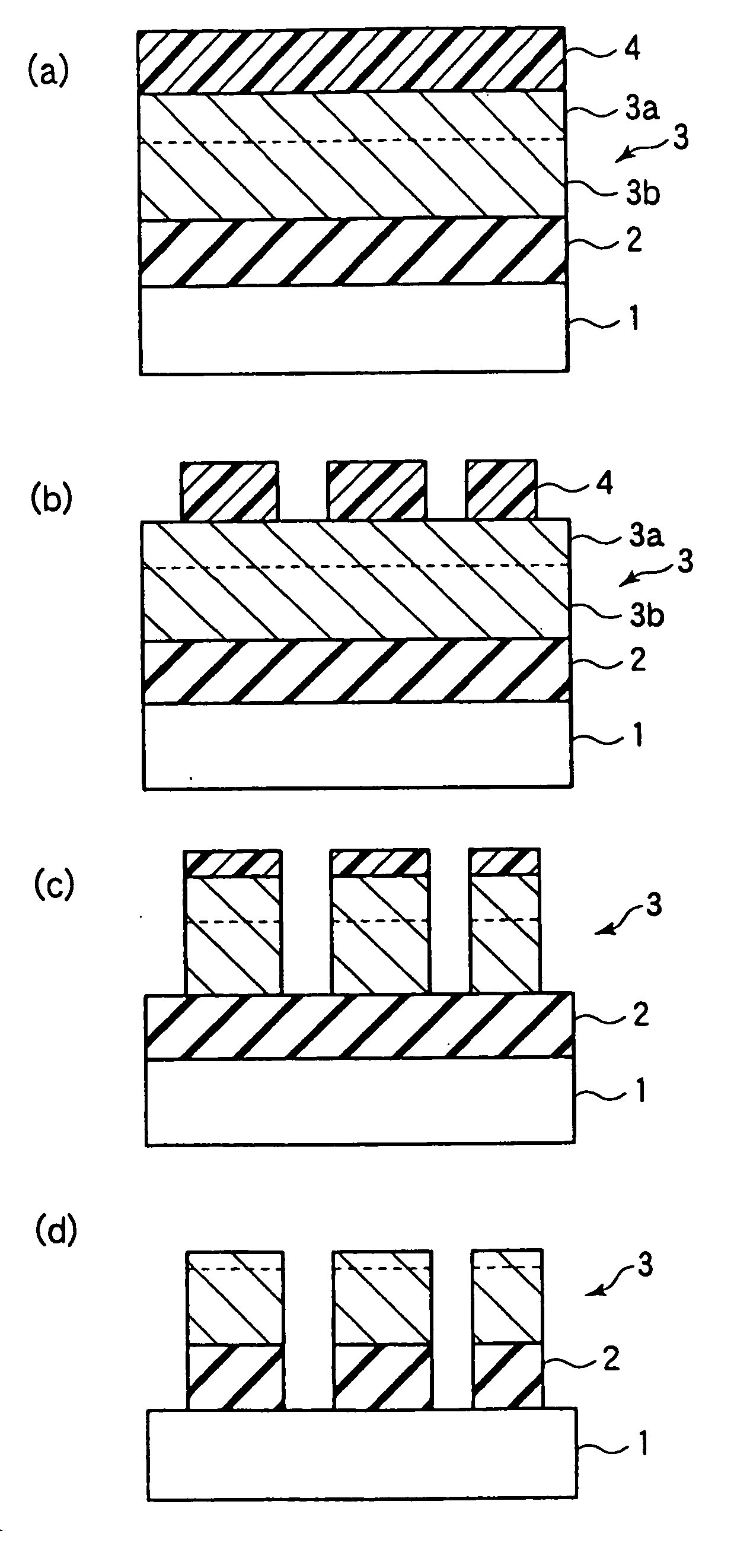
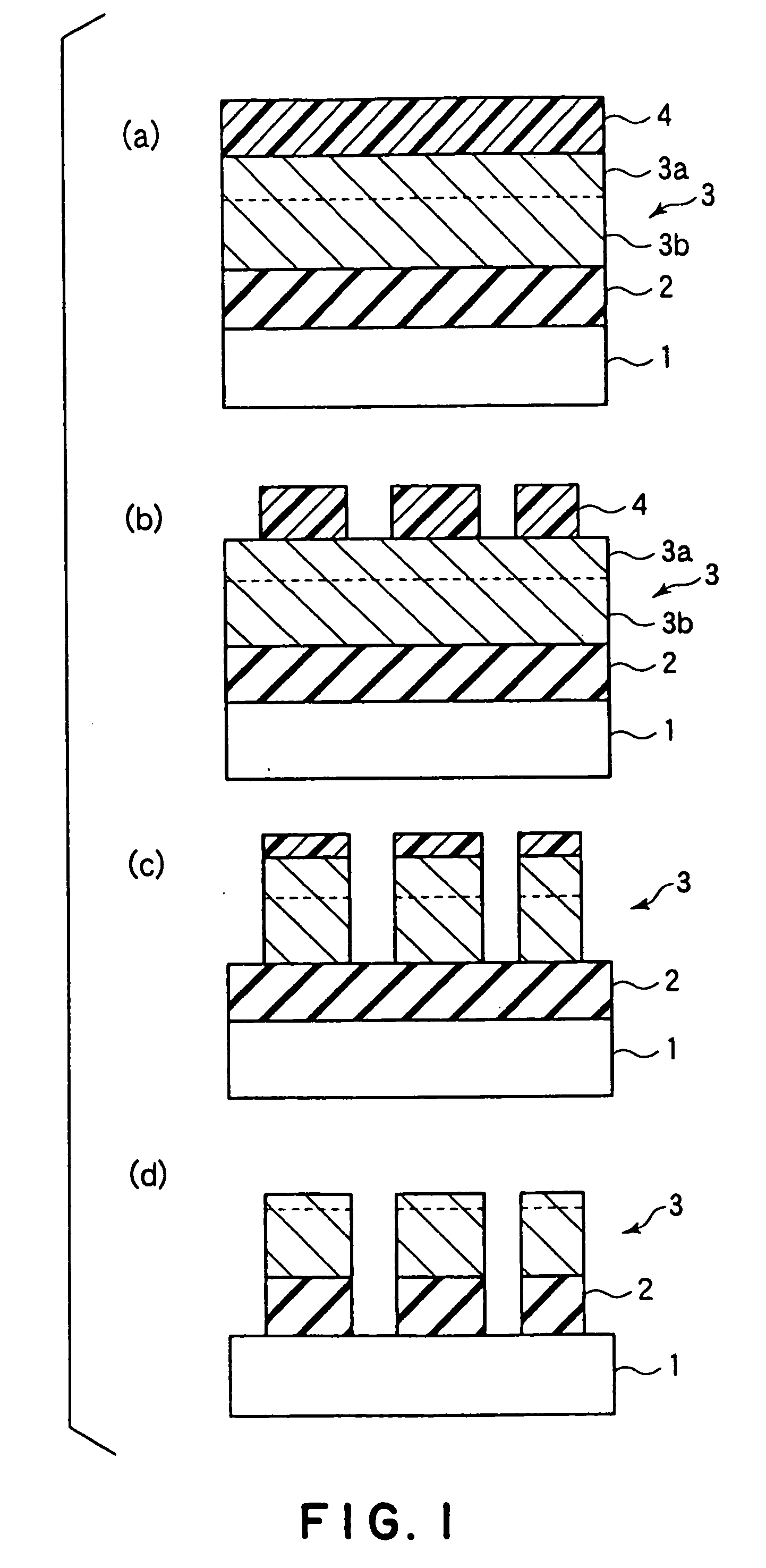
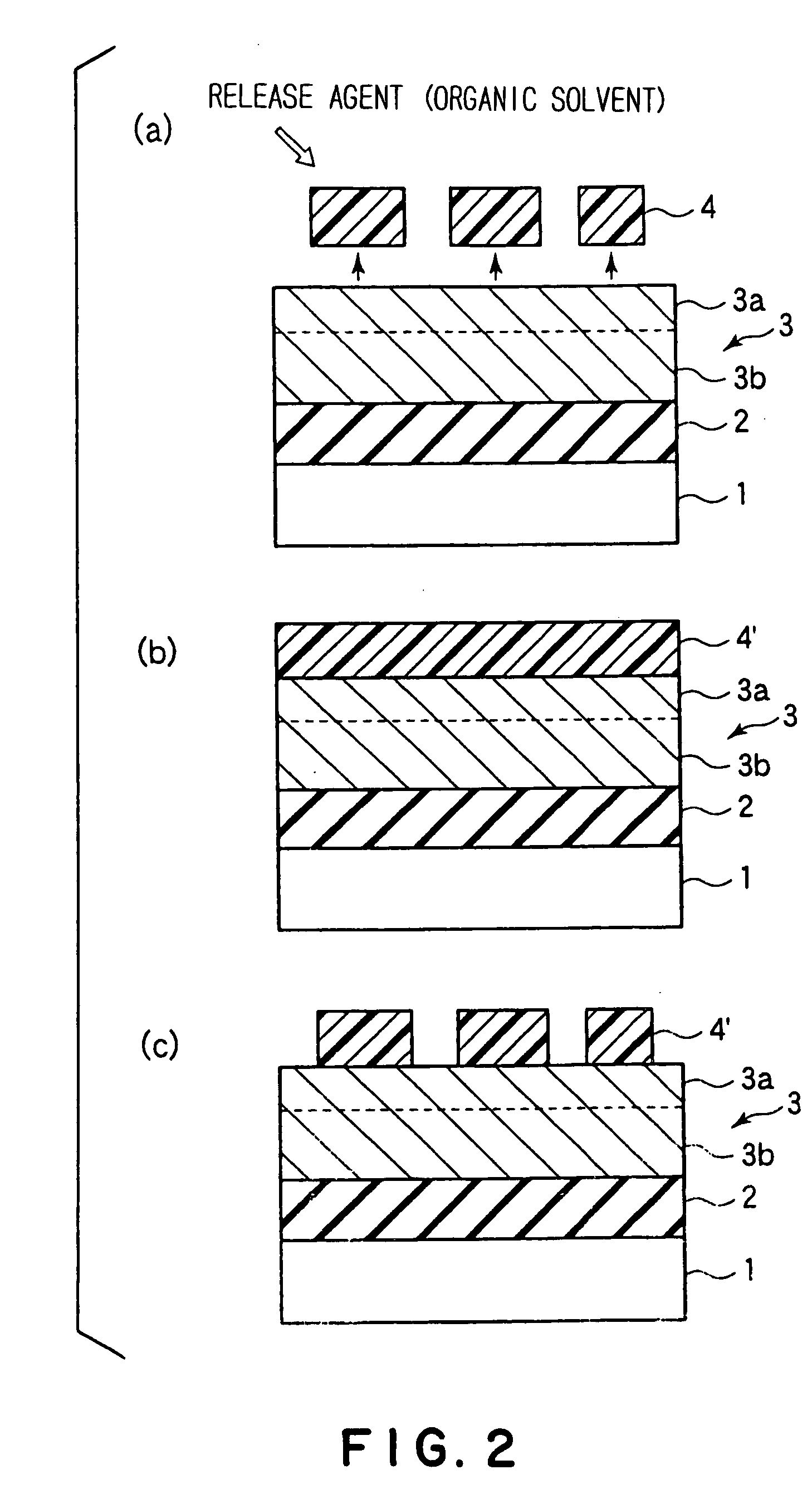
[0038]FIG. 1 shows schematic sectional views of a substrate for explanation of an etching method using an Si—C based film.

[0039] As shown in FIG. 1(a), an Si—C based film 3 is formed on an objective film to be etched 2, for example an oxide film (TEOS or a thermally oxidized film), which has been formed on a semiconductor substrate (semiconductor wafer) 1. A photo-resist film 4 is formed on the Si—C based film 3.

[0040] The Si—C based film 3 has an antireflection function and a hard-mask function. More specifically, the Si—C based film 3 is the same as that disclosed in the above document 1, which is available from IBM in the name of “TERA”. The Si—C based film 3 is a film of multi-layer structure formed by a plasma CVD process. Depending on materials of the objective film to be etched 2 and the photo-resist film 4, complex refractive index (n+ik: n is r...


PUM

PropertyMeasurementUnit
refractive indexaaaaaaaaaa
wavelengthaaaaaaaaaa

Abstract

A processing method of a substrate includes: a step of forming an Si—C based film and a resist film in turn on an objective film to be etched that has been formed on a substrate; a first etching step of etching the Si—C based film making use of the resist film as a mask; and a second etching step of etching the objective film to be etched making use of the resist film and the Si—C based film as a mask. The processing method further includes a peeling-off step of peeling-off the resist film at a desired timing. The peeling-off step includes a preparing step of preparing an organic solvent as a release agent, and an applying step of applying the organic solvent to the resist film.

Description

TECHNICAL FIELD [0001] The present invention relates to a peeling-off method and a reworking method of a resist film that has been formed onto an Si—C based film. BACKGROUND ART [0002] Recently, in forming a CMOS device, it has been requested to make thinner an antireflection film and a photo-resist film, which are used for an etching process, in order to achieve much finer structure. In particular, when an exposure apparatus with a high aperture ratio is used, it is more important to make thinner the photo-resist film. [0003] On the other hand, when the photo-resist film is made thinner, it may become difficult to accurately conduct an etching process. The problem may be taken into consideration for example when resist-trimming technique is used for achieving finer structure about a transistor gate length. In order to solve the problem, it has been proposed to introduce a hard mask under a photo-resist film / an antireflection film (ARC: Anti Reflective Coating). When this method is ...

Claims


Application Information

Patent Timeline
Patent Type & Authority Applications(United States)
IPC IPC(8): G03C1/00G03F7/42H01L21/00H01L21/027H01L21/304H01L21/311
CPCG03F7/42H01L21/67051H01L21/31144H01L21/31133H01J2237/3342
Inventor ASHIGAKI, SHIGEOKATO, YOSHIHIROHIROTA, YOSHIHIROMURAKI, YUSUKEKAWASAKI, TETSUSHIMURA, SATORU
Owner TOKYO ELECTRON LTD
Why Eureka
Try Eureka