Electronic imaging device with photosensor arrays

Inactive Publication Date: 2007-08-16
GE INSPECTION TECH
View PDF84 Cites 60 Cited by
  • Summary
  • Abstract
  • Description
  • Claims
  • Application Information

AI Technical Summary

Problems solved by technology

Often times, such a compromise sacrifices the best of both worlds, resulting in a dim image with poor depth of field.
Another drawback associated with conventional imagers aris

Method used


Image

  • Electronic imaging device with photosensor arrays
  • Electronic imaging device with photosensor arrays
  • Electronic imaging device with photosensor arrays

Examples


Embodiment Construction

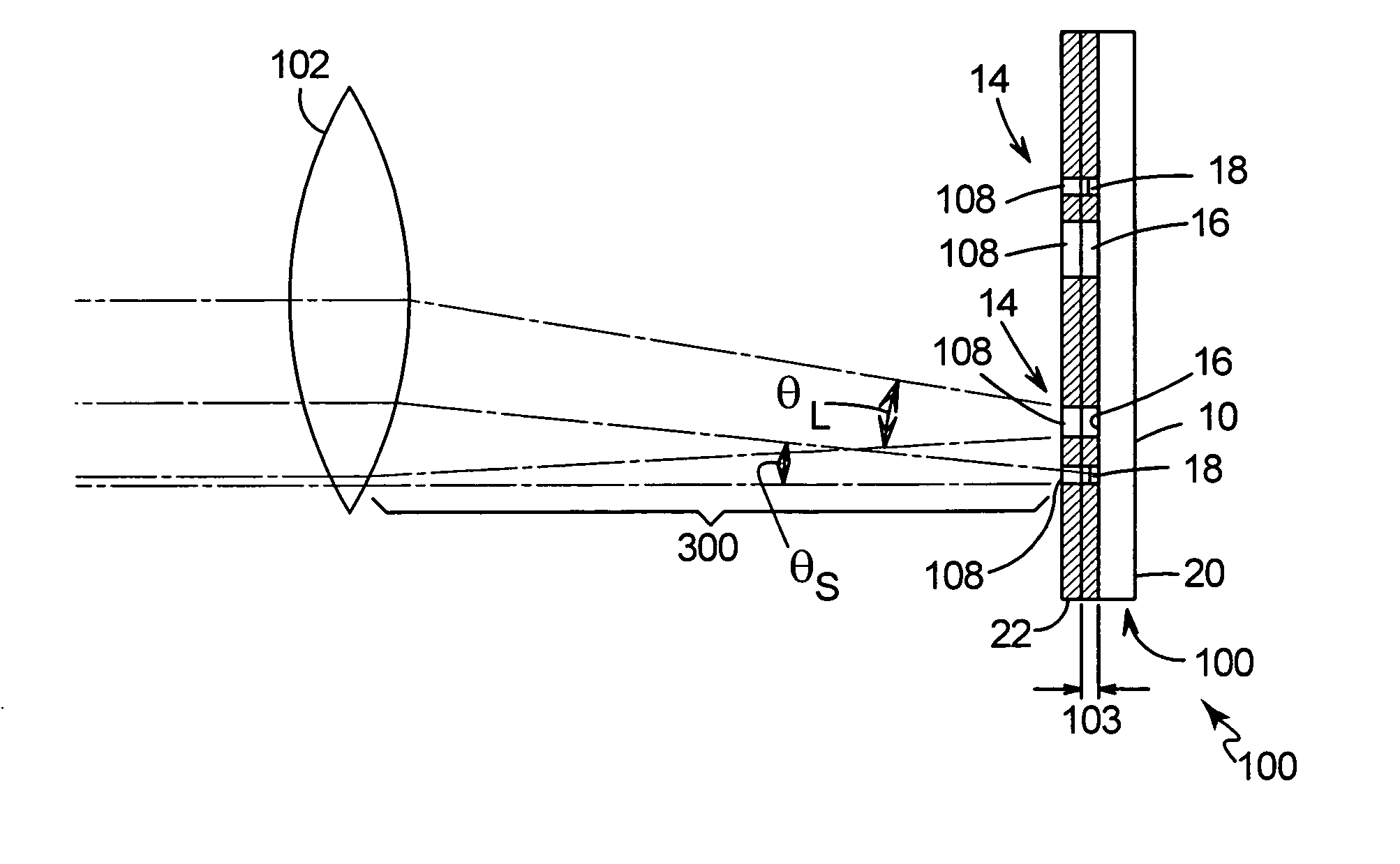
[0033]It is to be understood that the present application is not limited to the details of construction and arrangements of components that are set forth herein in the detailed description of the preferred embodiment(s), and / or that which is illustrated in the drawings. The embodiments depicted and described herein are capable of being practiced and / or being carried out in various ways. Reference will now be made in detail to currently preferred and other embodiments, examples of which are illustrated in the accompanying drawings. Whenever possible, the same reference numerals will be used throughout the drawings to refer to the same or like parts for clarity.

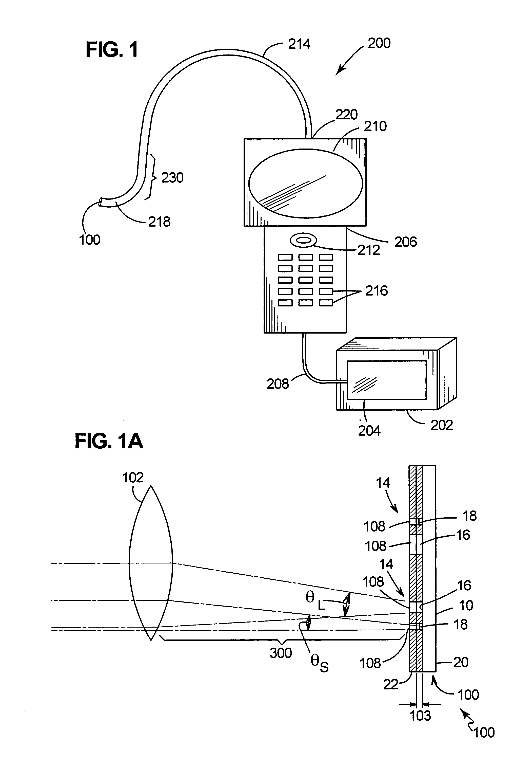
[0034]Referring to FIG. 1, an exemplary video imaging inspection device 200 (a borescope in the illustrative embodiment) is illustrated of the type commercially available, for example, from GE Inspection Technologies of Flanders, N.J. Such a device 200 could include, as shown in the illustrated embodiment, a portable shipping / o...


PUM


Abstract

An electronic imaging device is provided that includes a plurality of sensor elements, such as multiple photosensor arrays, wherein some of the sensor elements have a different numerical aperture value than the others, and wherein the sensor elements can be arranged such that their electrical signals can be combined to produce a composite electrical signal.

Description

CROSS REFERENCE TO RELATED APPLICATIONS[0001]This application claims priority from, and incorporates by reference the entirety of co-pending U.S. Provisional Patent Application Ser. No. 60 / 773,095, which was filed on Feb. 13, 2006.FIELD OF THE INVENTION[0002]The present invention relates generally to electronic imaging devices, and particularly to electronic imaging devices with multiple photosensor arrays.BACKGROUND OF THE INVENTION[0003]Traditional solid state imaging devices, such as those based on CCD (charge-coupled device) and CMOS (complementary metal oxide semiconductor) imaging devices, typically consist of a two-dimensional array of photosensors that are distributed on a surface or layer of a semiconductor chip, as well as an optical system used to focus an image (in the form of light passing through an aperture) onto the array. Each photosensor of the array commonly is generally referred to as a “picture element” or a “pixel.” The amount of light energy reaching each phot...

Claims


Application Information

Patent Timeline
IPC IPC(8): H01L27/00
CPCH04N5/2254H04N2005/2255H04N5/3696H04N5/335H04N23/555H04N25/00H04N25/702H04N23/843H04N25/134
Inventor LIA, RAYMOND A.
Owner GE INSPECTION TECH
Why Eureka
Try Eureka