
Asymmetric source/drain transistor employing selective epitaxial growth (SEG) layer and method of fabricating same

a technology of epitaxial growth and asymmetric source/drain transistor, which is applied in the field selective epitaxial growth (seg) layer, can solve the problems of reducing current driving capability, affecting the efficiency of asymmetric source/drain transistor, and difficult to control impurity ions that diffuse into the channel region, so as to improve the effect of short channel

Active Publication Date: 2007-08-16
SAMSUNG ELECTRONICS CO LTD
View PDF3 Cites 0 Cited by
  • Summary
  • Abstract
  • Description
  • Claims
  • Application Information

AI Technical Summary

Benefits of technology

[0011] One embodiment of the invention provides a method of fabricating an asymmetric source / drain transistor capable of improving a short channel effect by distributing channel ions asymmetrically.
[0012] Another embodiment of the invention provides a method of fabricating a transistor capable of distributing channel ions asymmetrically with ease.
[0013] Yet another embodiment of the invention provides an asymmetric source / drain transistor capable of distributing channel ions asymmetrically with ease.

Problems solved by technology

However, when the channel ions are doped to the high concentration, channel resistance increases so that current driving capability is decreased.
In particular, in a case where a capacitor stores charge, such as when a DRAM cell is connected to a source or a drain, the increase of the leakage current causes degradation of charge retention characteristics.
However, one drawback of forming the asymmetric channel region or the asymmetric source / drain regions with an ion implantation processes is that it is difficult to control impurity ions that diffuse into the channel region.

Method used


Image

  • Asymmetric source/drain transistor employing selective epitaxial growth (SEG) layer and method of fabricating same
  • Asymmetric source/drain transistor employing selective epitaxial growth (SEG) layer and method of fabricating same
  • Asymmetric source/drain transistor employing selective epitaxial growth (SEG) layer and method of fabricating same

Examples


Embodiment Construction

[0017] The invention is described below with reference to the accompanying drawings, in which exemplary embodiments of the invention are shown. In the drawings, the thickness of the layers and regions are exaggerated for clarity.

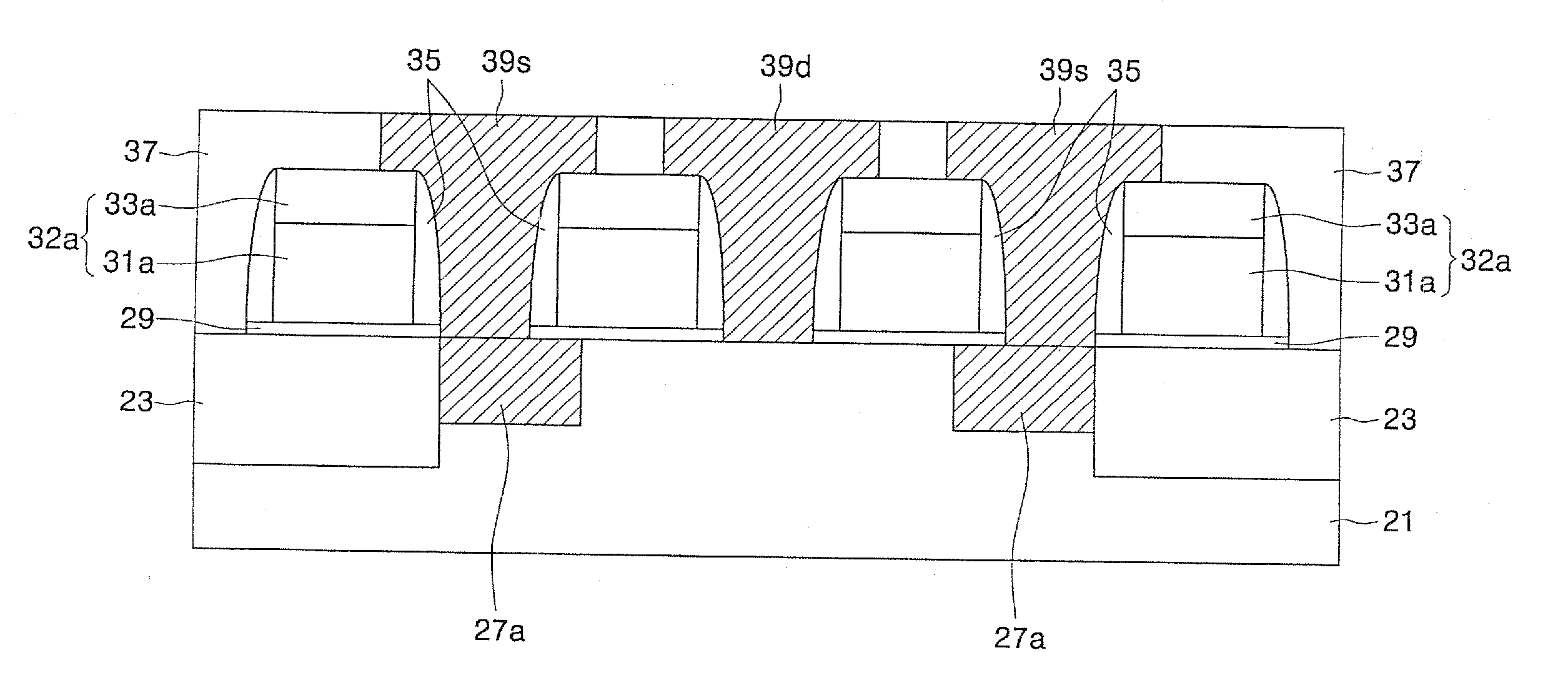
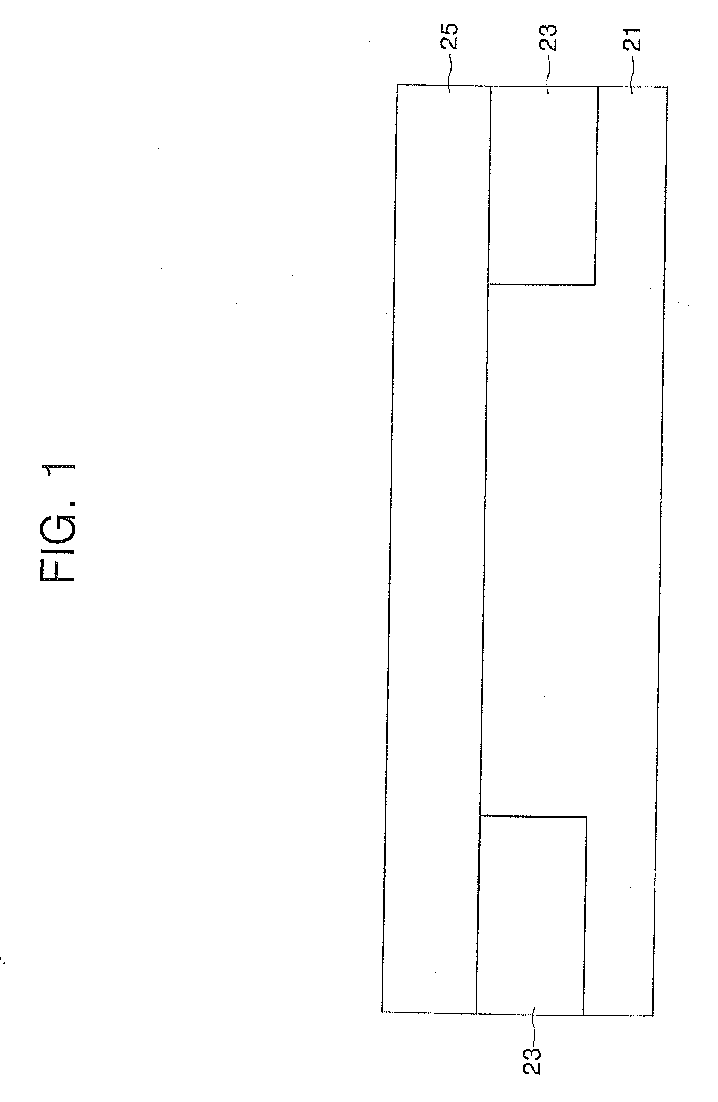
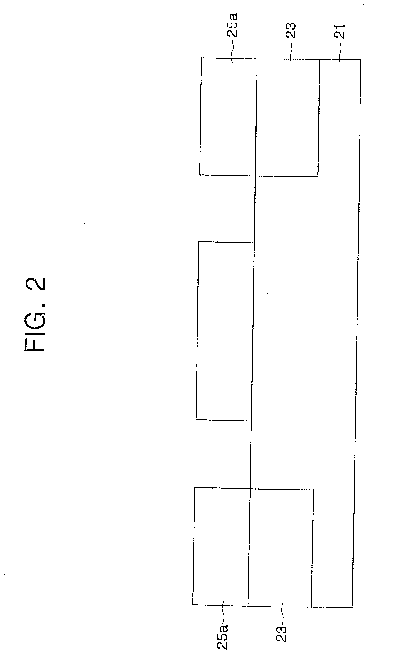
[0018] FIGS. 1 to 8 are cross-sectional diagrams illustrating a method of fabricating an asymmetric source / drain transistor in accordance with some embodiments of the invention.

[0019] Referring to FIG. 1, an isolation layer 23 for defining an active region is formed on a semiconductor substrate 21. The isolation layer 23 may be formed by a shallow trench isolation (STI) process.

[0020] Channel ions are doped on the semiconductor substrate having the isolation layer 23. The channel ions are distributed in the active region and may be N-type or P-type depending on what type of transistor is to be formed on the active region. That is, if the transistors to be formed on the active region are NMOS transistors and PMOS transistors, the channel ions are P-type an...


PUM


Abstract

According to some embodiments of the invention, a method includes preparing a semiconductor substrate having an active region, doping channel ions in the active region, forming a planarized selective epitaxial growth (SEG) layer in a predetermined region of the active region doped with the channel ions, sequentially forming a gate insulating layer, a gate conductive layer and a gate hard mask layer on the semiconductor substrate having the planarized SEG layer, forming a gate pattern crossing the active region by sequentially patterning the gate hard mask layer and the gate conductive layer, the planarized SEG layer being located at one side of the gate pattern, and forming source / drain regions by implanting impurity ions using the gate pattern as an ion implantation mask. Accordingly, there is provided an asymmetric source / drain transistor capable of preventing a leakage current by diffusing the channel ions into the SEG layer.

Description

CROSS REFERENCE TO RELATED APPLICATIONS [0001] This application is a divisional of U.S. patent application Ser. No. 11 / 067,410, filed 25 Feb. 2005, which claims priority from Korean Patent Application No. 2004-13684, filed 27 Feb. 2004, the contents of which are hereby incorporated by reference in their entirety for all purposes.BACKGROUND OF THE INVENTION [0002] 1. Field of the Invention [0003] This disclosure relates to a method of fabricating a semiconductor device and semiconductor device fabricated thereby and, more particularly, to a method of fabricating an asymmetric source / drain transistor employing a selective epitaxial growth (SEG) layer and asymmetric source / drain transistor fabricated thereby. [0004] 2. Description of the Related Art [0005] A semiconductor device generally employs a discrete device such as a MOS transistor as a switching device. As the degree of integration of the semiconductor device increases, the size of the MOS transistor decreases. As a result, the...

Claims


Application Information

Patent Timeline
Patent Type & Authority Applications(United States)
IPC IPC(8): H01L21/336H01L29/78
CPCH01L29/78H01L29/66636Y10S438/942A47G19/2227A47G21/04
Inventor SEO, HYEOUNG-WONSON, NAK-JINSONG, DU-HEONSEO, JUN
Owner SAMSUNG ELECTRONICS CO LTD
Learn More