METHOD FOR CONDUCTIVITY CONTROL OF (Al,In,Ga,B)N

a conductivity control and nitride technology, applied in the field of conductivity control of (al, in, ga, b) n, can solve the problems of reduced oscillator strength, red-shifted emission, and restricted carrier recombination efficiency, and achieve the effect of improving the conductivity of semipolar nitride semiconductor crystals

Active Publication Date: 2007-08-16
RGT UNIV OF CALIFORNIA
View PDF17 Cites 115 Cited by
  • Summary
  • Abstract
  • Description
  • Claims
  • Application Information

AI Technical Summary

Benefits of technology

[0038] The method may further comprise performing a subsequent thermal annealing step, after the deposition step, which alters a concentration of unintentional impurity

Problems solved by technology

However, conventional c-plane quantum well structures in III-nitride based optoelectronic and electronic devices suffer from the undesirable quantum-confined Stark effect (QCSE), due to the existence of strong piezoelectric and spontaneous polarizations.
The strong built-in electric fields along the c-direction cause spatial separation of electrons and holes that in turn give rise to restricted carrier recombination efficiency, reduced oscillator strength, and r

Method used


Image

  • METHOD FOR CONDUCTIVITY CONTROL OF (Al,In,Ga,B)N
  • METHOD FOR CONDUCTIVITY CONTROL OF (Al,In,Ga,B)N
  • METHOD FOR CONDUCTIVITY CONTROL OF (Al,In,Ga,B)N

Examples


Embodiment Construction

[0048] In the following description of the preferred embodiment, reference is made to the accompanying drawings which form a part hereof, and in which is shown by way of illustration a specific embodiment in which the invention may be practiced. It is to be understood that other embodiments may be utilized and structural changes may be made without departing from the scope of the present invention.

[0049] Overview

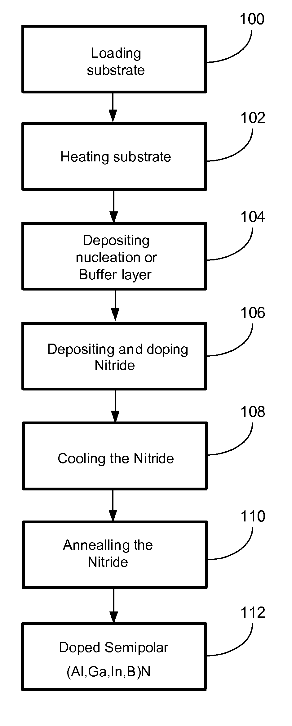
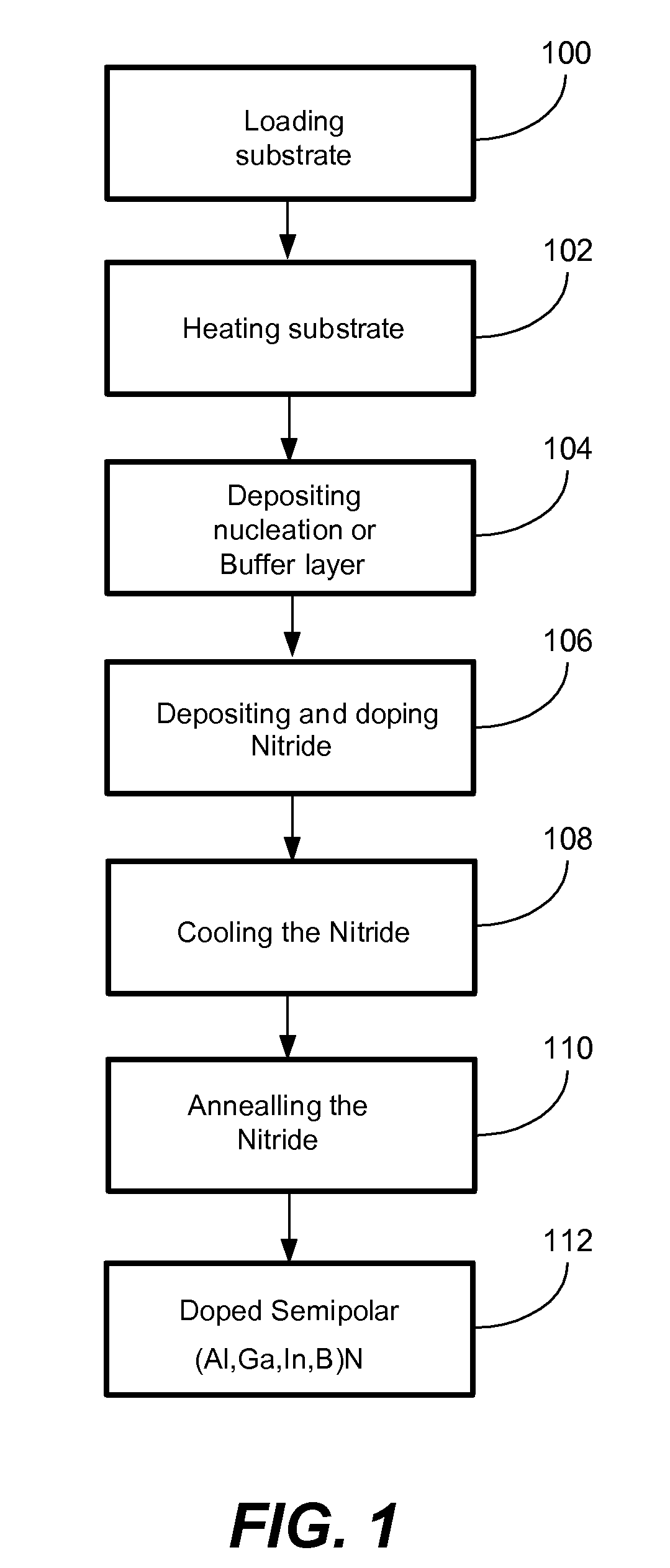
[0050] The present invention comprises a method of controlled p-type conductivity in (Al,In,Ga,B)N semiconductor crystals by doping of a semipolar nitride crystal. Examples of such control have been demonstrated using {10 11} GaN films deposited on {100} MgAl2O4 spinel substrates miscut in the direction. In one embodiment of the invention, magnesium atoms are intentionally incorporated in the growing semipolar nitride film to introduce available electronic states in the band structure of the semiconductor crystal, resulting in p-type conductivity. Other impurity atoms, su...


PUM


Abstract

A method of controlled p-type conductivity in (Al,In,Ga,B)N semiconductor crystals. Examples include {10 11} GaN films deposited on {100} MgAl2O4 spinel substrate miscut in the <011> direction. Mg atoms may be intentionally incorporated in the growing semipolar nitride thin film to introduce available electronic states in the band structure of the semiconductor crystal, resulting in p-type conductivity. Other impurity atoms, such as Zn or C, which result in a similar introduction of suitable electronic states, may also be used.

Description

CROSS-REFERENCE TO RELATED APPLICATIONS [0001] This application claims the benefit under 35 U.S.C. Section 119(e) of the following co-pending and commonly-assigned U.S. patent application: [0002] U.S. Provisional Patent Application Ser. No. 60 / 772,184, filed on Feb. 10, 2006 John F. Kaeding, Hitoshi Sato, Michael Iza, Hirokuni Asamizu, Hong Zhong, Steven P. DenBaars and Shuji Nakamura entitled “METHOD FOR CONDUCTIVITY CONTROL OF SEMIPOLAR (Al,In,Ga,B)N”, attorneys docket number 30794.166-US-P1 (2006-285); [0003] which application is incorporated by reference herein. [0004] This application is related to the following co-pending and commonly-assigned applications: [0005] U.S. Utility patent application Ser. No. 11 / 372,914 filed Mar. 10, 2006, by Troy J. Baker, Benjamin A. Haskell, Paul T. Fini, Steven P. DenBaars, James S. Speck, and Shuji Nakamura, entitled “TECHNIQUE FOR THE GROWTH OF PLANAR SEMI-POLAR GALLIUM NITRIDE,” attorneys docket number 30794.128-US-U1 (2005-471), which appl...

Claims


Application Information

Patent Timeline
IPC IPC(8): H01L21/04H01L29/15
CPCH01L21/0242H01L21/02433H01L21/0254H01L21/02579H01L21/2654H01L21/0262H01L29/045H01L29/2003H01L29/207H01L21/02609H01L21/04H01L29/15H01L21/20
Inventor KAEDING, JOHN F.SATO, HITOSHIIZA, MICHAELASAMIZU, HIROKUNIZHONG, HONGDENBAARS, STEVEN P.NAKAMURA, SHUJI
Owner RGT UNIV OF CALIFORNIA
Why Eureka
Try Eureka