Method for forming electrodes and/or black stripes for plasma display substrate

a plasma display substrate and electrode technology, applied in the manufacture of electrode systems, cold cathode manufacturing, electric discharge tubes/lamps, etc., can solve the problems of high cost, increased resistivity of ito, and high cost of ito, so as to reduce the risk of eroding, reduce the cost, and reduce the effect of eroding

Inactive Publication Date: 2007-08-16
ASAHI GLASS CO LTD
View PDF6 Cites 22 Cited by
  • Summary
  • Abstract
  • Description
  • Claims
  • Application Information

AI Technical Summary

Benefits of technology

[0031] According to the present invention, display electrodes made of ITO, bus electrodes employing Ag or Cr / Cu / Cr and optional black stripes employing a black dielectric, for a plasma display substrate, which used to be produced by using different materials respectively, can be formed of the same material which is inexpensive, has a low resistance and is less susceptible to erosion by a dielectric, and further, it is possible to provide a method for forming electrodes and / or black stripes for a plasma display substrate, capable of displaying a clear image on a PDP display device.
[0032] Further, according to the present invention, as compared with a conventional wet system such as a photolithography / etching process or a wet lift-off method, it is possible to form electrodes and / or black stripes for a plasma display substrate in a smaller number of process steps at lower costs. Further, it is a dry method employing a laser beam, whereby it is unnecessary to use a large amount of a chemical liquid such as a developer or an etching agent as in the wet method, and it is unnecessary to worry so much about a load on the environment such as waste liquid treatment which has becomes a serious concern recently.

Problems solved by technology

However, ITO is expensive.
Further, in PDP of the AC type, if ITO is covered with a dielectric, the dielectric is likely to erode ITO, and the resistivity of ITO is likely to be thereby increased.
However, in such a case, the original purposes of the dielectric, such as the insulation performance and the performance to prevent erosion from plasma, are likely to decrease at the same time.
Accordingly, the production process is long and expensive, and a strong acid or a strong alkaline solution is employed, whereby the load to the environment is large.

Method used


Image

  • Method for forming electrodes and/or black stripes for plasma display substrate
  • Method for forming electrodes and/or black stripes for plasma display substrate
  • Method for forming electrodes and/or black stripes for plasma display substrate

Examples


embodiment

[0166] Now, the present invention will be described in further detail with reference to an Embodiment, but it should be understood that the present invention is by no means thereby restricted.

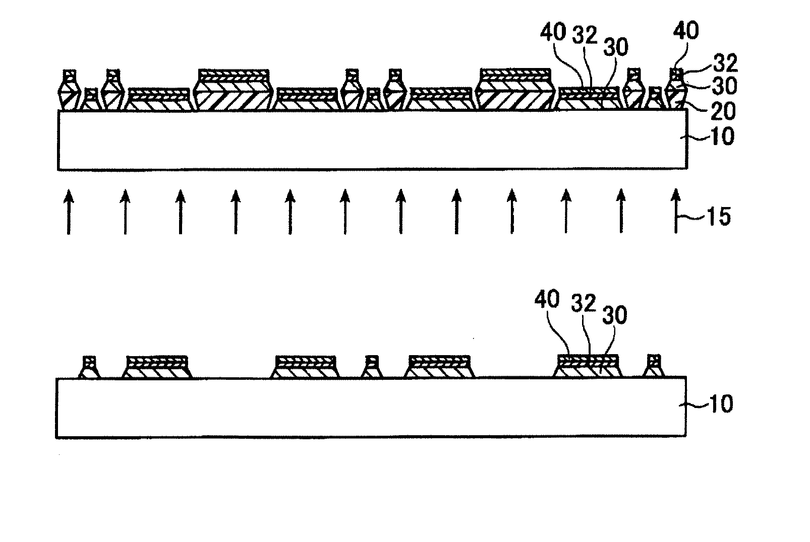
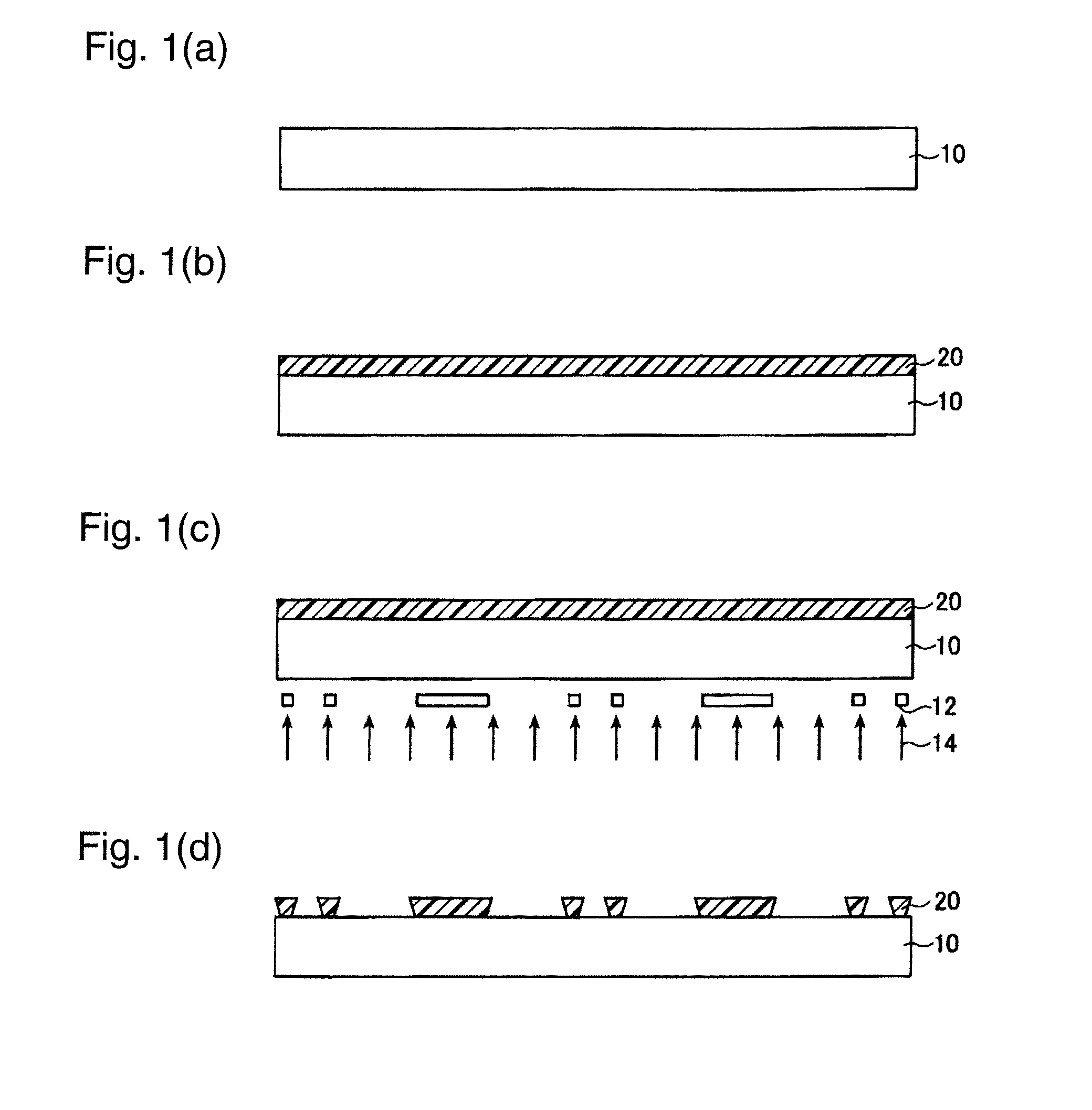
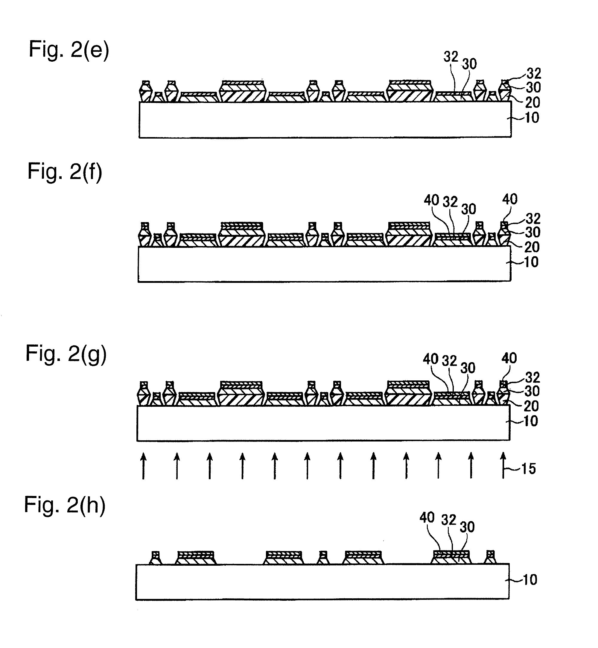
[0167] The method for forming electrodes and / or black stripes for a plasma display substrate according to the Embodiment will be described with reference to FIGS. 8 to 10.

[0168] In this Embodiment, as the mask layer, a film made of a mask layer-forming material of an acrylic resin containing 40 mass % of carbon black (hereinafter referred to simply as “a mask film”) is used; as the first antireflection layer-forming material, metal Cr (purity: at least 99.99%) is used; as the second antireflection layer-forming material, metal Cr (purity: at least 99.99%) is used; as the electrode layer-forming material, metal copper (purity: at least 99.99%) is used; and as the protective layer-forming material, metal Cr (purity: at least 99.99%) is used.

[0169] The mask film as well as the first antireflect...


PUM


Abstract

To provide a method for forming electrodes and / or black stripes for a plasma display substrate, wherein display electrodes, bus electrodes and optionally black stripes for a plasma display panel are formed of the same material by the same dry step, whereby a clear image having reflection prevented, can be displayed on a PDP display device with a low load on the environment, at low costs, with low resistance, without erosion by a dielectric. A method for forming electrodes and / or black stripes for a plasma display substrate, which comprises applying a laser beam to a mask layer formed on a transparent substrate to form openings at areas corresponding to the respective patterns of display electrodes, bus electrodes and optionally black stripes, then continuously forming an antireflection layer to provide an antireflection effect over the entire surface and an electrode layer, and applying again a laser beam to peel off the mask layer and at the same time to remove an unnecessary thin film layer.

Description

TECHNICAL FIELD [0001] The present invention relates to a method for forming electrodes and / or black stripes for a plasma display substrate; a plasma display substrate provided with electrodes and / or black stripes, thereby formed; and a plasma display panel employing it. BACKGROUND ART [0002] A plasma display panel (hereinafter referred to also as “PDP”) can be made thin and easily large-sized and further has characteristics such as light weight, high resolution, etc., and thus, it has attracted attention as a prospective candidate to be substituted for CRT as a display device. [0003] PDP is generally classified into a DC type and an AC type, but its operational principle is one utilizing a light emission phenomenon due to gas discharge. For example, in the AC type, as shown in FIG. 11, cells (spaces) are defined by partition walls 3 formed between a transparent front substrate 1 and a rear substrate 2 facing each other, and in the cells, a Penning mixed gas such as He+Xe or Ne+Xe h...

Claims


Application Information

Patent Timeline
Patent Type & Authority Applications(United States)
IPC IPC(8): H01J9/24H01J9/00H01J17/04H01J17/49
CPCH01J9/02H01J11/12H01J2211/444H01J11/44H01J11/22H01J9/20
Inventor SATOH, RYOHEIIWATA, YOSHINORINAKAGAWA, KOJITANAKA, KENJITAKAKI, SATORU
Owner ASAHI GLASS CO LTD
Why Eureka
Try Eureka