Method of manufacturing an inlet member for an electronic tag

a manufacturing method and electronic tag technology, applied in the direction of instruments, circuit masks, resonant antennas, etc., can solve the problems of high process cost, high manufacturing cost of this kind of electronic tag, and high spread of electronic tag, and achieve the effect of accurately and cheaply formed

Inactive Publication Date: 2007-08-23
RENESAS TECH CORP
View PDF6 Cites 4 Cited by
  • Summary
  • Abstract
  • Description
  • Claims
  • Application Information

AI Technical Summary

Benefits of technology

[0034] That is, the pattern of the antenna of the inlet

Problems solved by technology

However, since structure is complicated compared with the tag using a bar code etc., the manufacturing cost of this kind of electronic tag is high, and this constitutes a cause which bars the spread of electronic tags.
This technology has the problem that process cost is high, from the material cost of polyimide resin and copper

Method used


Image

  • Method of manufacturing an inlet member for an electronic tag
  • Method of manufacturing an inlet member for an electronic tag
  • Method of manufacturing an inlet member for an electronic tag

Examples


Embodiment Construction

[0052] Hereafter, embodiments of the invention are explained in detail based on drawings. In all the drawings for describing the embodiments, members of the same function will be identified by the same reference numerals in principle and overlapping descriptions will be omitted.

[0053] The inlet for electronic tags of this embodiment (it is only hereafter described as an inlet) forms the main part of the noncontact type electronic tag provided with the antenna for microwave reception.

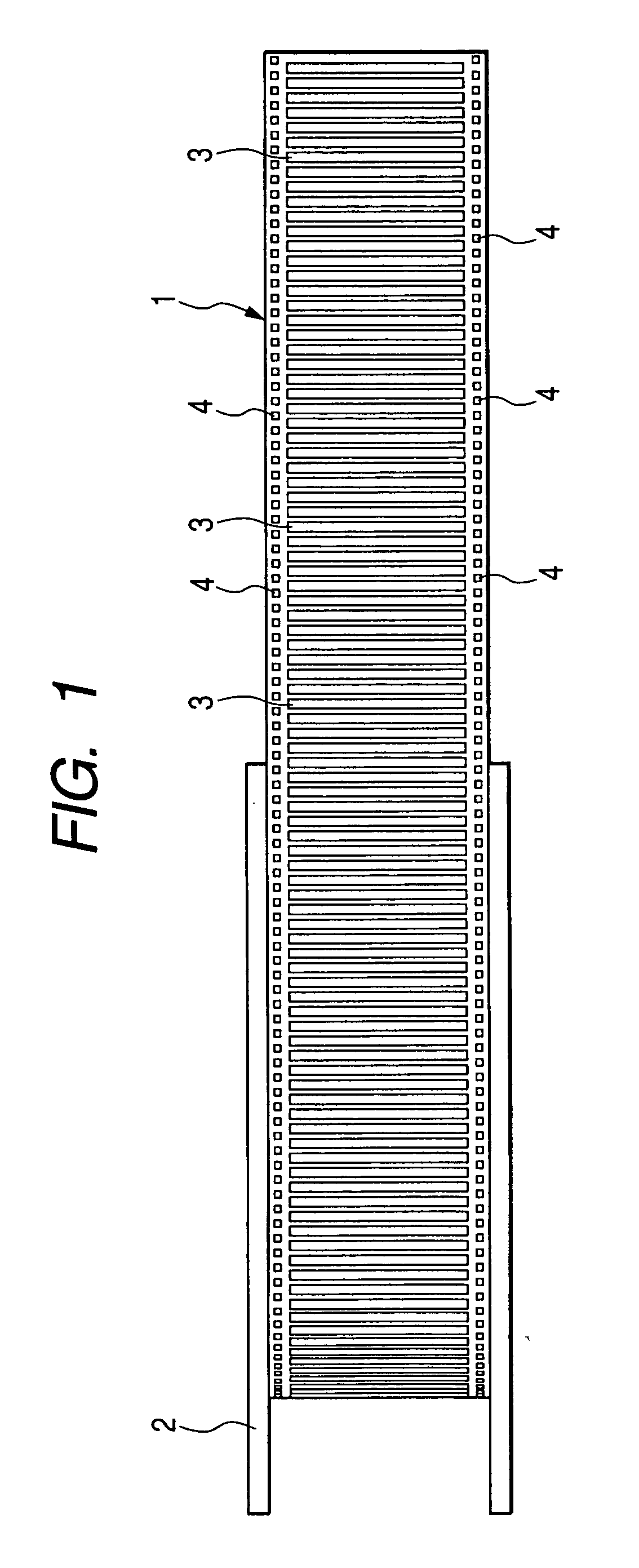
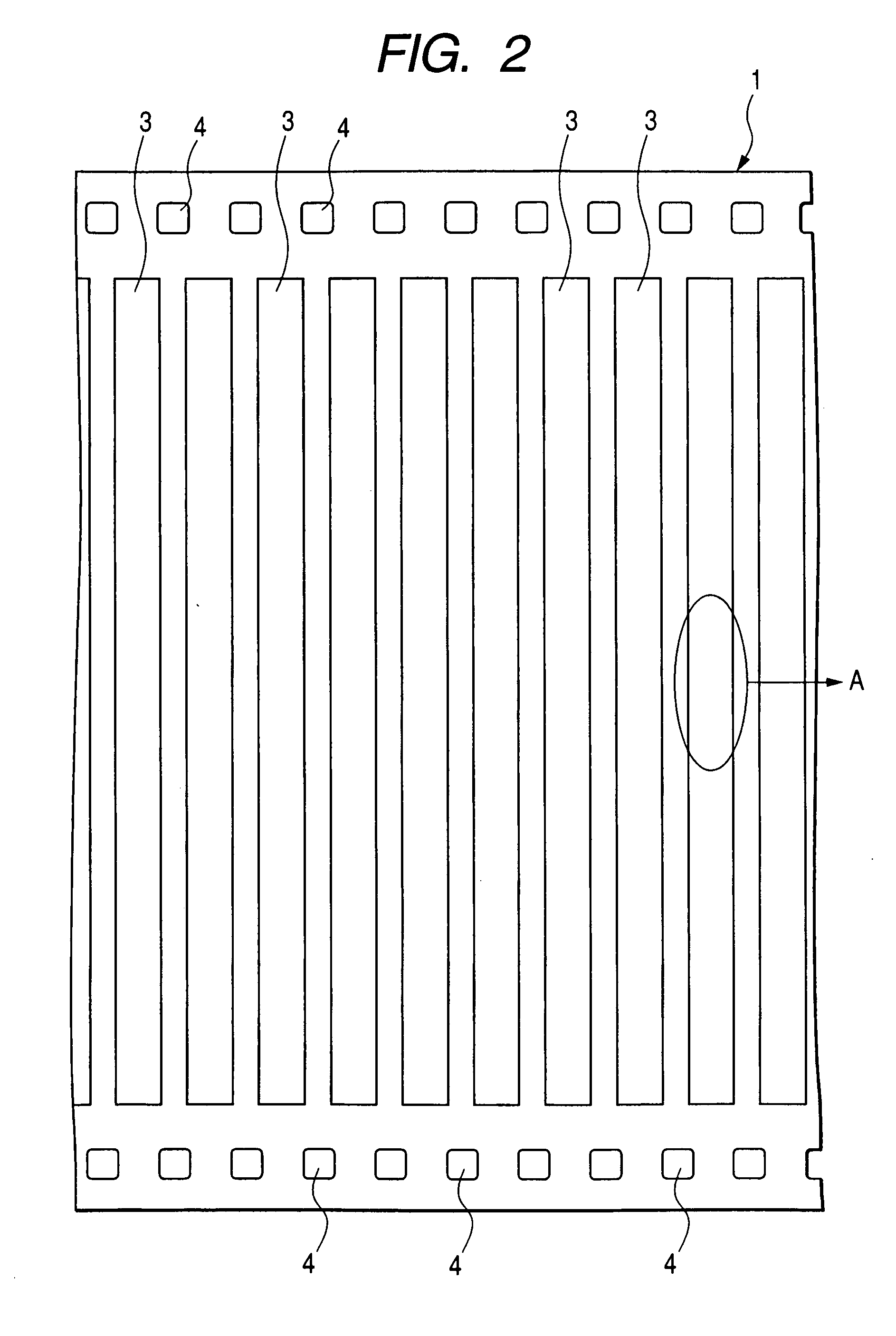
[0054]FIG. 1 is a plan view showing insulating film 1 used for manufacture of the inlet of this embodiment, and FIG. 2 is a plan view expanding and showing an part of FIG. 1.

[0055] As shown in FIG. 1 and FIG. 2, insulating film 1 is carried in to the manufacturing process of the inlet of this embodiment after having been rolled round by reel 2. Many antennas 3 are beforehand formed in one side of this insulating film 1 at the predetermined gap. In this embodiment, insulating film 1 is formed, for exam...


PUM

PropertyMeasurementUnit
Angleaaaaaaaaaa
Angleaaaaaaaaaa
Electric chargeaaaaaaaaaa

Abstract

In order to offer the technology which can form the pattern of the antenna of the inlet for electronic tags accurately and cheaply, the resist layer at the time of forming the pattern of an antenna by chemical etching is formed using a photogravure printing machine. Let the extending direction of region 16C which has the minimum width in the height of the front surface of a gravure plate be an opposite direction to the direction of rotation of a gravure plate (a doctor's relative direction of movement seen from the gravure plate). The radius of curvature of an inner circumference of the curved part in region 16B is made larger than the radius of curvature of a periphery. The outer edge of region 16D is formed so that it may become forward tapered shape-like toward position D, so that the width of region 16D may become larger than the width of region 16C in position D which the end of height attains.

Description

INCORPORATION BY REFERENCE [0001] The present application claims priority from PCT application PCT / JP2005 / 000467 filed on Jan. 17, 2005, the content of which is hereby incorporated by reference into this application. TECHNICAL FIELD [0002] The present invention relates to a manufacturing technology of an inlet for noncontact type electronic tags, and particularly relates to an effective technology in the application to a patterning step of an antenna. BACKGROUND ART [0003] For example, in when using conductor ink and forming the circuit pattern comprising a thin wire wiring part by a gravure method on a base material, there is technology which can form cheaply the circuit pattern comprising a thin wire wiring part by forming a printing plate with a direct printing method, forming the machine plate which surface-mounted the pattern of the thin wire wiring part to perpendicular direction or oblique direction to the doctor's direction, and doing gravure of the resist pattern of the cir...

Claims


Application Information

Patent Timeline
IPC IPC(8): H01P11/00G06K19/00G06K19/077H01Q1/22H01Q9/16H05K3/00H05K3/06
CPCG06K19/07718Y10T29/49018G06K19/07756H01L2224/16H01L2924/01004H01L2924/01046H01L2924/01078H01L2924/01079H01Q1/2208H05K3/0076H05K3/061H05K2203/0113H05K2203/0143Y10T29/49016Y10T29/4913G06K19/07749H01L2224/05022H01L2224/05001H01L2224/05572H01L2224/051H01L2224/05664H01L2224/05666H01L24/05H01L24/13H01L2924/00014
Inventor MORINAGA, YUICHIIKEDA, YUJISAKAMOTO, SHINTARO
Owner RENESAS TECH CORP
Why Eureka
Try Eureka