Optoelectric composite substrate and electronic apparatus

a technology of optoelectric composite substrates and electronic devices, which is applied in the direction of optical elements, semiconductor lasers, instruments, etc., can solve the problems of difficult to make the planar area of the molded section, the molded section described above cannot be larger than the area, and it is difficult in the fresnel region to convert the laser beam into parallel light or to condense the laser beam

Inactive Publication Date: 2007-08-23
SEIKO EPSON CORP
View PDF5 Cites 29 Cited by
  • Summary
  • Abstract
  • Description
  • Claims
  • Application Information

AI Technical Summary

Benefits of technology

[0009]In view of the above circumstances, an advantage of the invention is to provide an optoelectric composite substrate capable of preventing degradation of the production yield caused by damages of a molded section without causing an elevation of the production cost, and an electronic apparatus equipped with the optoelectric composite substrate.
[0010]According to an aspect of the invention, an optoelectric composite substrate includes a substrate; a light emitting element positioned on the substrate; and a lens mold positioned on the light emitting element and contacting at least a part of the substrate. The lens mold includes a lens element, the lens element positions so as to overlap an emitting surface of the light emitting element, and a distance between the light emitting element and the lens element is greater than a range of a Fresnel region of the light emitting element.
[0011]In the optoelectric composite substrate a distance between the light emitting element and the lens element is preferably within a range of a Fraunhofer region of the light emitting element. According to this aspect of the invention, in the case in which the surface of the lens mold is formed inside the Fraunhofer region, and the lens element is formed on the surface, the lens surface can be formed without causing elevation of the manufacturing cost.
[0012]In the optoelectric composite substrate assuming that a diameter of a near-field pattern of the light emitted by the light emitting element is D and a wavelength thereof is λ, a Fraunhofer region of the light emitted from the light emitting element is preferably an area with a greater distance from the light emitting element than the distance L=D2 / λ. It should be noted that the diameter D is a rough diameter of an area drawn by a plot satisfying maximum intensity of the intensity distribution of the near-field pattern multiplied by (1 / e raised to the power 2).
[0013]In the optoelectric composite substrate, the light emitting element is a VCSEL, and the Fresnel region is preferably a distance between an active layer of VCSEL and the lens element.
[0014]In the optoelectric composite substrate, an electric circuit is disposed on the substrate, the electric circuit is electrically connected to the light emitting element via a wiring pattern, and a part of the electric circuit preferably contacts the lens mold.

Problems solved by technology

Meanwhile, according to the above document, since a microlens is formed directly on gallium arsenide (GaAs) substrate provided with VCSEL, it is difficult to make the planar area of a molded section including a microlens greater than the planar area of VCSEL chip divided later.
Therefore, there is a restriction that the molded section described above cannot be made larger than the area obtained by subtracting the planar area of the electrode from the planar area of VCSEL chip.
Although fairing of the laser beam by a lens or the like is possible in the Fraunhofer region, it is quite difficult in the Fresnel region to convert the laser beam into parallel light or to condense the laser beam.
Considering the two restrictions described above, if the planar area of VCSEL chip is about 500 μm square, it is quite difficult to provide the base area of the molded section forming a microlens sufficiently with respect to the height thereof as disclosed in the document mentioned above.
Therefore, it is easily conceivable that damages such as breakage, slant, uncoupling, or bend of the molded section might be caused in a dicing process for clipping the discrete VCSEL, from the substrate, which causes degradation of production yield.
Although enlargement of the base area (the contact area with the substrate) of the molded section is effective for preventing such damages, if the base area of the molded section is enlarged, the size of the discrete VCSEL chip becomes remarkably large to significantly reduce the number of VCSEL chips manufactured from one sheet of the substrate, thus causing an elevation of the production cost.

Method used


Image

  • Optoelectric composite substrate and electronic apparatus
  • Optoelectric composite substrate and electronic apparatus
  • Optoelectric composite substrate and electronic apparatus

Examples


first embodiment

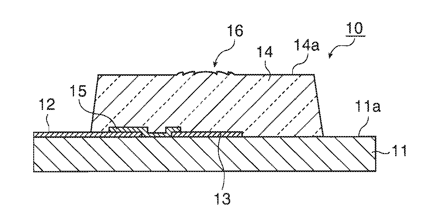
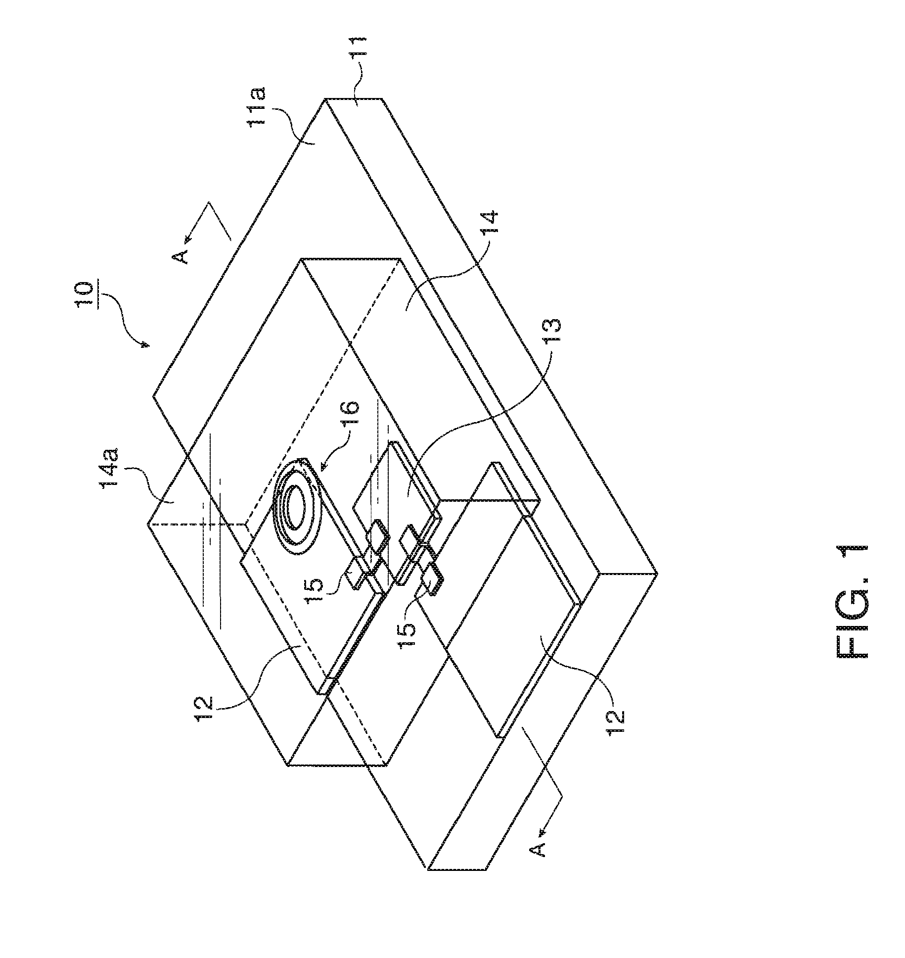
[0060]FIG. 1 is a perspective view showing a substantial part of an optoelectric composite substrate 10 according to a first embodiment of the invention, and FIG. 2 is a cross-sectional view along the A-A line shown in FIG. 1. As shown in FIGS. 1 and 2, the optoelectric composite substrate 10 is configured including a substrate 11, a printed wiring pattern 12 formed on a side of the front face 11a of the substrate 11, a low-profile optical element 13 mounted on the side of the front face 11a of the substrate 11, and a lens mold 14 formed on the side of the front face 11a of the substrate 11 so as to cover the top of the low-profile optical element 13. It should be noted that although in the present embodiment, the case in which the optoelectric composite substrate 10 is a printed wiring board with very little flexibility is explained as an example, it can be a flexible printed wiring board (FPC) with much flexibility.

[0061]As the substrate 11, a substrate made at least of, for examp...

second embodiment

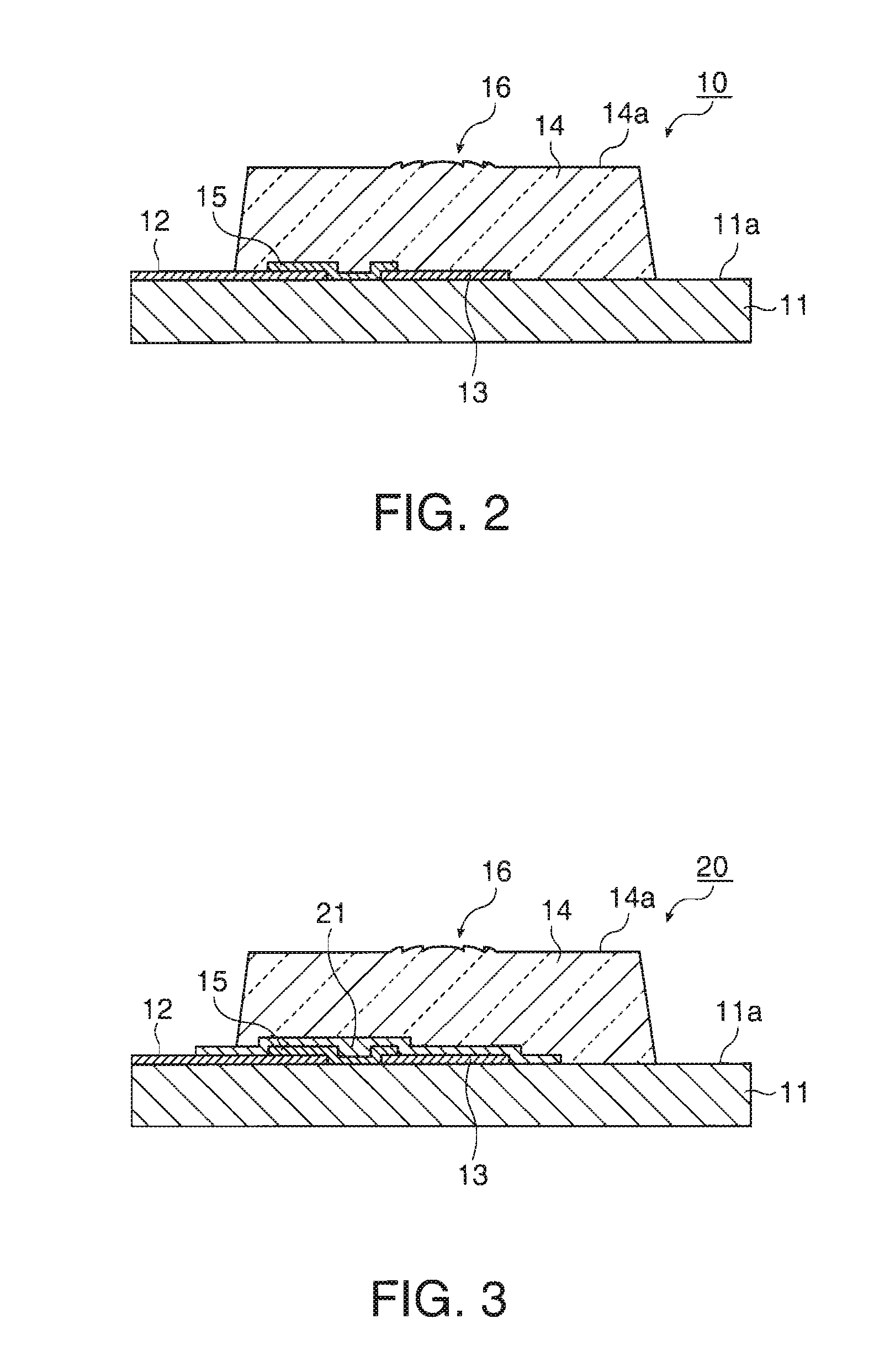
[0082]FIG. 4 is a cross-sectional view showing a substantial part of the optoelectric composite substrate according to a second embodiment of the invention. It should be noted that the components corresponding to the components provided to the optoelectric composite substrate 10 according to the first embodiment explained using the FIGS. 1 and 2 are denoted with the same reference numerals. As shown in FIG. 4, an optoelectric composite substrate 30 is configured including a substrate 31, the low-profile optical element 13 mounted on the side of the front face 31a of the substrate 31, and a lens mold 34 formed on the side of the front face 31a of the substrate 31 so as to cover the top of the low-profile optical element 13. It should be noted that although wiring patterns corresponding to the printed wiring patterns 12 provided to the optoelectric composite substrate 10 shown in FIGS. 1 and 2 are not illustrated in the example shown in FIG. 4, these wiring patterns can be formed on t...

third embodiment

[0089]FIG. 5 is a cross-sectional view showing a substantial part of the optoelectric composite substrate according to a third embodiment of the invention. It should be noted that the components corresponding to the components provided to the optoelectric composite substrate 30 according to the second embodiment explained using the FIG. 4 are denoted with the same reference numerals. Comparing an optoelectric composite substrate 40 of the present embodiment shown in FIG. 5 with the optoelectric composite substrate 30 of the second embodiment shown in FIG. 4, they are different from each other in that a new low-profile optical element 43 is mounted on the front face 31a of the substrate 31, and the lens elements 36a, 36b are formed on the front face 34a of the lens mold 34 respectively corresponding to the low-profile optical elements 13, 43. It should be noted that in the present embodiment, it is assumed that the low-profile optical element 13 is a light emitting element such as a ...


PUM

PropertyMeasurementUnit
thicknessaaaaaaaaaa
thicknessaaaaaaaaaa
thicknessaaaaaaaaaa

Abstract

An optoelectric composite substrate includes a substrate, a light emitting element positioned on the substrate, and a lens mold positioned on the light emitting element and contacting at least a part of the substrate, wherein the lens mold includes a lens element, the lens element positions so as to overlap an emitting surface of the light emitting element, and a distance between the light emitting element and the lens element is greater than a range of a Fresnel region of the light emitting element.

Description

BACKGROUND OF THE INVENTION[0001]1. Technical Field[0002]Several aspects of the present invention relate to an optoelectric composite substrate equipped with an electric wiring pattern and a photoelectric transducer, and an electronic apparatus equipped with the optoelectric composite substrate.[0003]2. Related Art[0004]In recent years, optical communications for performing transmission / reception of information using optical signals have been in heavy usage. The optical communications have advantages such as lower attenuation, increased amount of handling information, or prevention of electromagnetic irradiation to the environment in comparison with electrical communications for performing transmission / reception of information using electric signals. Although in the past the optical communications have been almost limited to middle / long distance communications of longer than about several hundreds of kilometers, in recent years they have been frequently used for short-range communic...

Claims


Application Information

Patent Timeline
Patent Type & Authority Applications(United States)
IPC IPC(8): H01L33/00G02B1/04H01S5/183
CPCH01L25/167H01L2924/3011H01L2924/09701H01L33/54H01L24/83H01L24/95H01L2224/83001H01L2224/83192H01L2924/0002H01L2924/12041H01L2924/00
Inventor KONDO, TAKAYUKI
Owner SEIKO EPSON CORP
Why Eureka
Try Eureka