

Method For Manufacturing Semiconductor Device
- Summary
- Abstract
- Description
- Claims
- Application Information
AI Technical Summary
Benefits of technology
Problems solved by technology
Method used
Image

Examples
embodiment mode 1
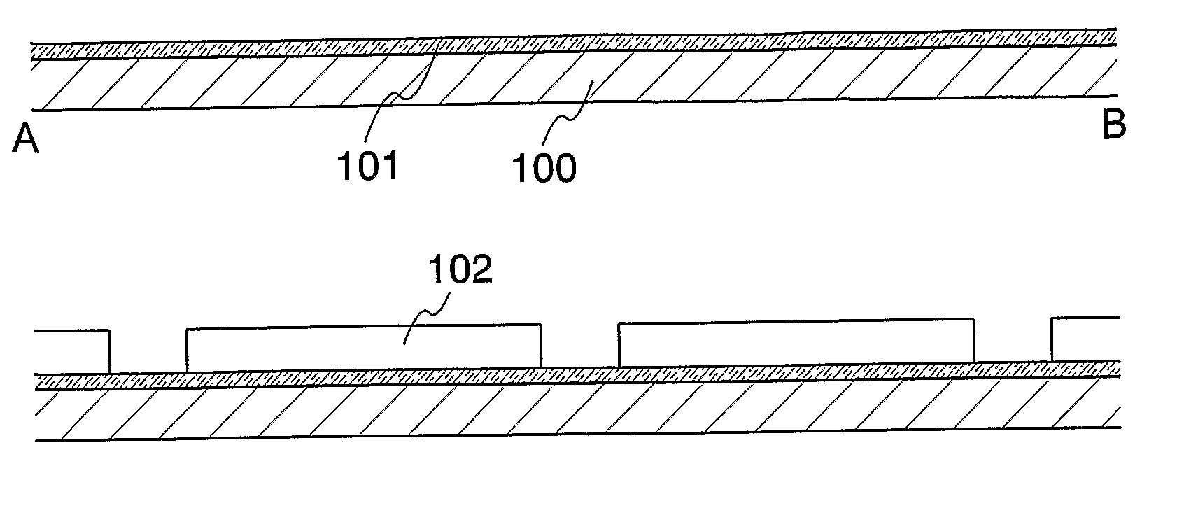
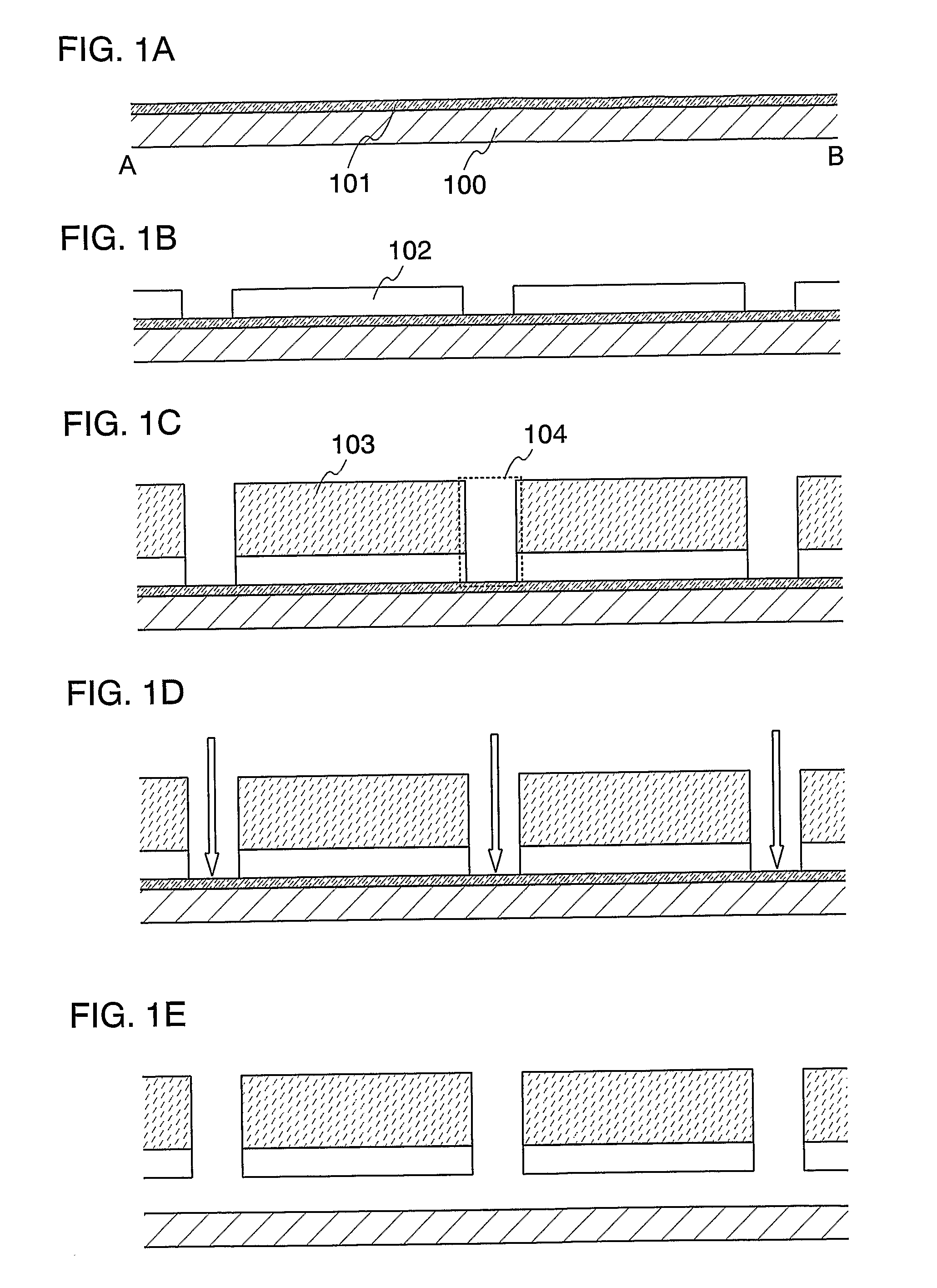
[0055] In this embodiment mode, a method for separating a thin film integrated circuit provided over a substrate from the substrate will be explained. Here, the case of providing a plurality of integrated circuits over a substrate and then separating the plurality of integrated circuits from the substrate will be explained with reference to drawings.
[0056] First, a substrate 100 is prepared and a release layer 101 is formed over the substrate 100 as shown in FIG. 1A. Specifically, a glass substrate of, for example, barium borosilicate glass, aluminoborosilicate glass, a quartz substrate, a ceramic substrate, or the like can be used as the substrate 100. Further, a substrate of metal of such as stainless steel or a semiconductor substrate provided with an insulating film on its surface may also be used. Although a substrate made of a flexible synthetic, such as plastics, generally tends to have lower heat-resistance than the above-described substrate, it can be used as the substrate...
embodiment mode 2
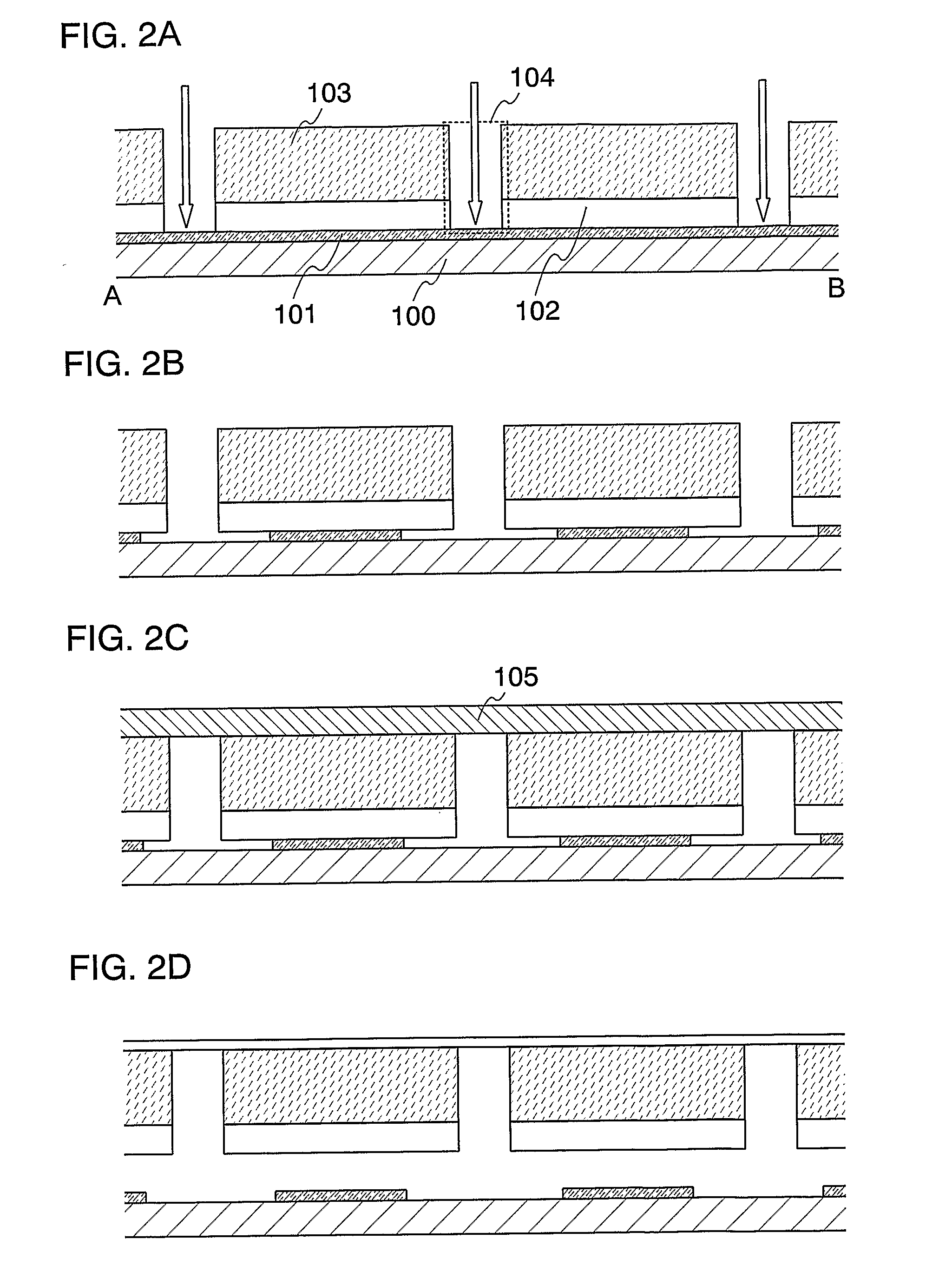
[0071] In this embodiment mode, a method for separating a thin film integrated circuit provided over a substrate from the substrate, which is different from that in Embodiment Mode 1, will be explained with reference to FIGS. 2A to 2D.
[0072] In this embodiment mode, steps shown in figures up to FIG. 1C can be carried out in the same manner as Embodiment Mode 1. Accordingly, the materials and the structure described in Embodiment Mode 1 are used in the steps shown in figures up to FIG. 2A.
[0073] Thereafter, in this embodiment mode, an etchant is introduced into the opening 104 (FIG. 2A), and at least a part of the release layer disposed below the TFT layer 102 is left without completely removing the release layer 101 (FIG. 2B). How much of the release layer is left can be controlled by setting an etching flow rate and reaction time in consideration of reaction of the release layer with the etchant. Any material described in Embodiment Mode 1 can be used for the release layer. Note ...
embodiment mode 3
[0083] In this embodiment mode, a method for separating a thin film integrated circuit provided over a substrate from the substrate, which is different from those in the above embodiment modes, will be explained with reference to drawings. Specifically, explained is the case where a thin film integrated circuit is formed over a substrate with a release layer having an opening therebetween, and the release layer is removed, thereby peeling by a physical means the substrate and the thin film integrated circuit from each other which are attached to each other in the opening.
[0084] First, a release layer 101 is formed over the substrate 100 as previously shown in FIG. 1A (FIG. 4A).
[0085] Next, the release layer 101 is etched using a photolithography technique to form a pattern having a plurality of openings 106 (FIG. 4B). Alternatively, a pattern may be formed by forming a resist by a droplet discharge method and etching the same. The droplet discharge method is a method for selective...
PUM
 Abstract
Description
Claims
Application Information