Modulator apparatus operating at low supply voltage, and corresponding method of modulation

a technology of low supply voltage and modulator, which is applied in the direction of modulator-demodulator, dc amplifier, analog and hybrid computing, etc., can solve the problems of requiring very low supply voltage, limiting the development of modern sub-micrometric technologies, and not enabling a very contained power dissipation

Active Publication Date: 2007-08-30
STMICROELECTRONICS INT NV
View PDF3 Cites 35 Cited by
  • Summary
  • Abstract
  • Description
  • Claims
  • Application Information

AI Technical Summary

Benefits of technology

[0025] One embodiment of the present invention solves the drawbacks described above and proposes a solution that enables operation with a low value of minimum supply voltage and at low consumption levels, controlling way the gain in a precise, in particular in a way that presents low sensitivity in regard to the phenomenon of channel modulation.

Problems solved by technology

Said requirements are met via the use of high-efficiency CMOS technological processes with sub-micrometric channel lengths, which, however, on account of certain technological constraints, require very low supply voltages.
In addition, the minimum value of supply voltage VDDmin that guarantees operation of said circuit topology is rather high, and this constitutes an even more limiting factor for modern sub-micrometric technologies.
It hence follows that, even though the circuit topology of FIG. 2 is suitable for low-supply-voltage applications, it does not enable a very contained power dissipation, which is a fundamental parameter for portable applications.
On the other hand, however, it presents a series of disadvantages that reduce the aforesaid advantages in the actual definition of the circuit.
Said elements unfavorably affect the transfer of signal and determine a lack of accuracy of the conversion gain of the modulator apparatus; this represents in general a limit for completely integrated circuit applications.
Furthermore, even though the effect of channel modulation can be mitigated by the use of long-channel MOS devices, since the constraints on the input and output dynamic ranges (low overdrive→high shape ratio W / L) impose the use of high shape factors, this results in large parasitic capacitances at the drains of the transistors M2a″ and M2b″, with consequent high feed-through of the local oscillator.

Method used


Image

  • Modulator apparatus operating at low supply voltage, and corresponding method of modulation
  • Modulator apparatus operating at low supply voltage, and corresponding method of modulation
  • Modulator apparatus operating at low supply voltage, and corresponding method of modulation

Examples


Embodiment Construction

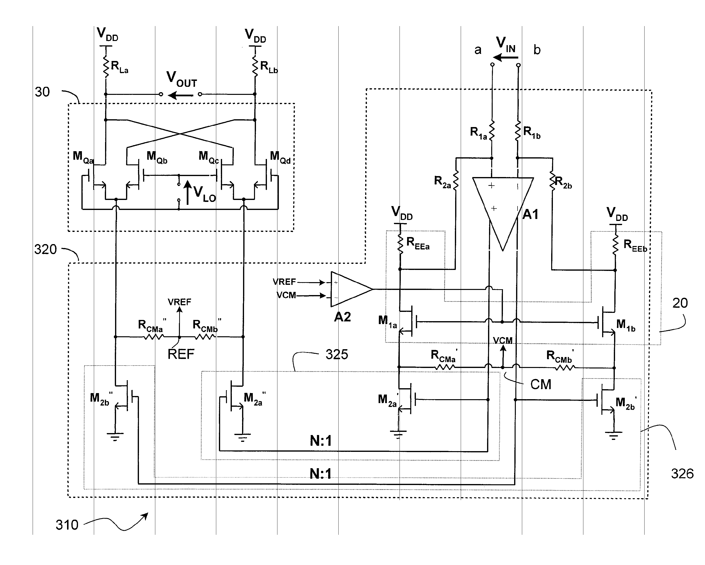
[0030] In brief, a modulator apparatus and a corresponding method of modulation are proposed, which envisage providing in the transconductor stage a feedback of a differential type for reproducing the input signal on the differential load, and a common-mode feedback so that the gain of the current mirror will be extremely accurate and will behave equivalently to a cascode mirror.

[0031]FIG. 4 represents a circuit implementation of the modulator apparatus proposed, designated as a whole by the reference number 310.

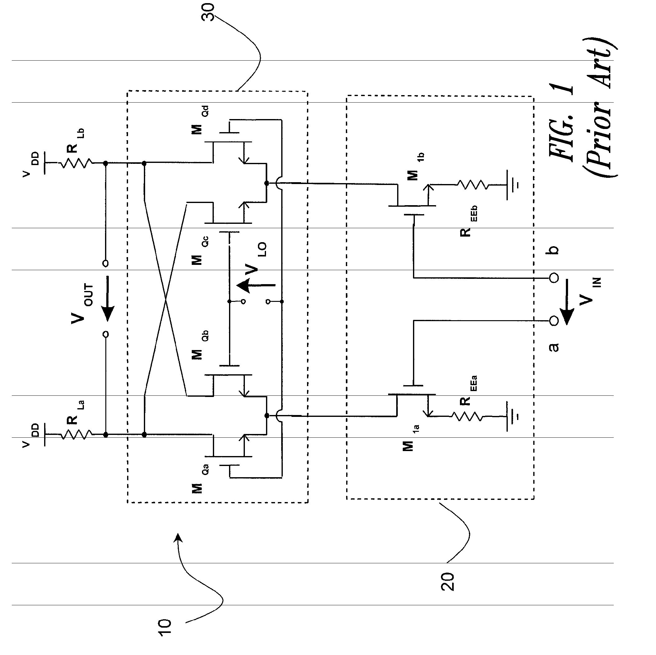
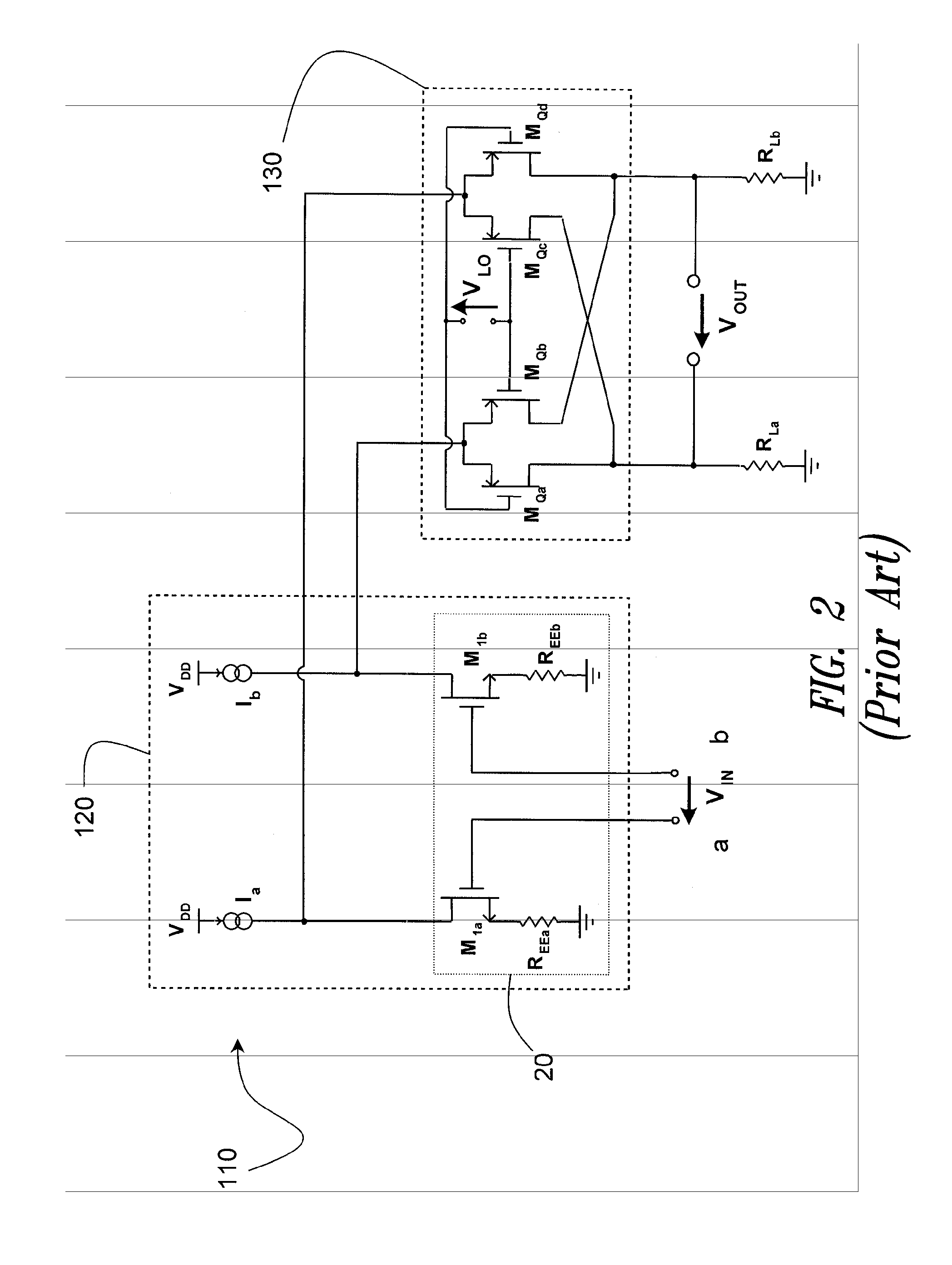
[0032] Said modulator apparatus 310 comprises a transconductor stage 320, which carries out the voltage-to-current conversion of the input-voltage signal Vin supplied by the base-band circuit. Associated to the output of the transconductor stage 320 is a Gilbert cell 30, similar to the ones shown in FIGS. 1 and 3. Said Gilbert cell 30, stimulated by the control signal VLO coming from a local oscillator, which is not shown here either, carries out the conversion to the high...


PUM


Abstract

A modulator apparatus operating at a low supply voltage, configured for receiving an input-voltage signal in base band and supplying an output-voltage signal at a given modulation frequency under control of a signal generated by a local oscillator and comprising a transconductor stage that carries out a voltage-to-current conversion of said input-voltage signal. A voltage-to-current conversion module is coupled to a current-mirror module configured for mirroring a current in a Gilbert-cell stage, which supplies an output-voltage signal under the control of said signal generated by the local oscillator. The Gilbert-cell stage further comprises an output load for carrying out a current-to-voltage conversion and supplying the output-voltage signal. Said transconductor stage further comprises a differential feedback network configured for reproducing said input-voltage signal on a differential load included in said voltage-to-current conversion module.

Description

BACKGROUND OF THE INVENTION [0001] 1. Field of the Invention [0002] The present description relates to apparatuses and methods for modulation of base-band signals into signals operating at given frequencies, in particular radio-frequency. [0003] 2. Description of the Related Art [0004] The tendency of the market of microelectronic devices of presenting increasingly high levels of performance at extremely contained costs, as well as the concentration of an increasingly higher number of functions in portable devices, intensifies the demand for devices that involve a low power consumption. Said requirements are met via the use of high-efficiency CMOS technological processes with sub-micrometric channel lengths, which, however, on account of certain technological constraints, require very low supply voltages. All of these elements have in general a marked impact on the design of analog circuits, and frequently impose the use of non-conventional structures. [0005] One of the circuit bloc...

Claims


Application Information

Patent Timeline
Patent Type & Authority Applications(United States)
IPC IPC(8): H03F3/38
CPCH03D7/1441H03D2200/0084H03F3/45475H03F3/45632H03F2200/513H03F2203/45008H03F2203/45028H03F2203/45074H03F2203/45078H03F2203/45082H03F2203/45136H03F2203/45418H03F2203/45424H03F2203/45541H03F2203/45542H03F2203/45588H03F2203/45594H03F2203/45644H03F2203/45652H03D7/1433H03D7/1458H03D2200/0025H03D2200/0033H03F3/45192
Inventor FILORAMO, PIETROCAVALLARO, ALBERTOCHIARILLO, TIZIANO
Owner STMICROELECTRONICS INT NV
Why Eureka
Try Eureka