Wafer level package for very small footprint and low profile white LED devices

Active Publication Date: 2007-08-30
GE LIGHTING SOLUTIONS LLC
View PDF11 Cites 115 Cited by
  • Summary
  • Abstract
  • Description
  • Claims
  • Application Information

AI Technical Summary

Benefits of technology

[0006] In such a package, the thickness of the LED chip after substrate removal is very thin (typically less than 5 microns) relative to its lateral dimension. Therefore, side emission of light is minimal, and the phosphor coating is suitably optionally limited to the tops of the LED chips. The phosphor layer is optionally supported by the chip and underfill outside the chips without coating the submount. Alternatively, the phosphor can coat both the LED chips and the laterally intervening submount areas. By bonding individual chips close together and supporting them by underfill material, the host submount c

Problems solved by technology

Therefore, side emission of light is minimal, and the phosphor co

Method used


Image

  • Wafer level package for very small footprint and low profile white LED devices
  • Wafer level package for very small footprint and low profile white LED devices
  • Wafer level package for very small footprint and low profile white LED devices

Examples


Embodiment Construction

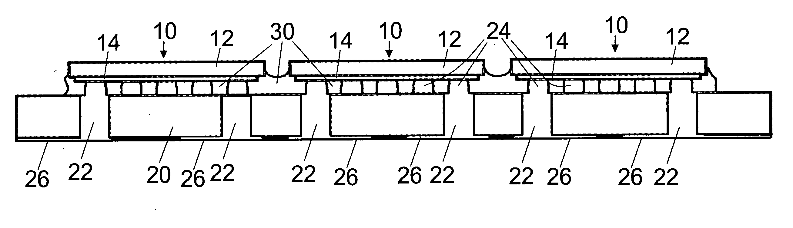
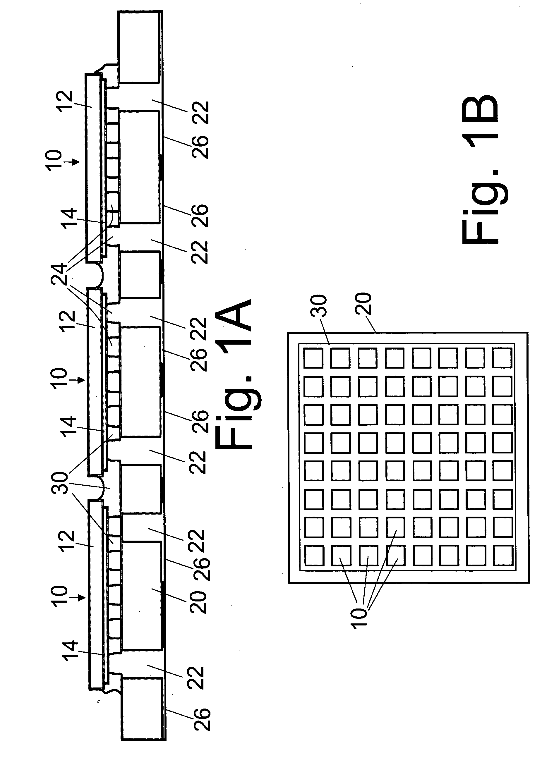
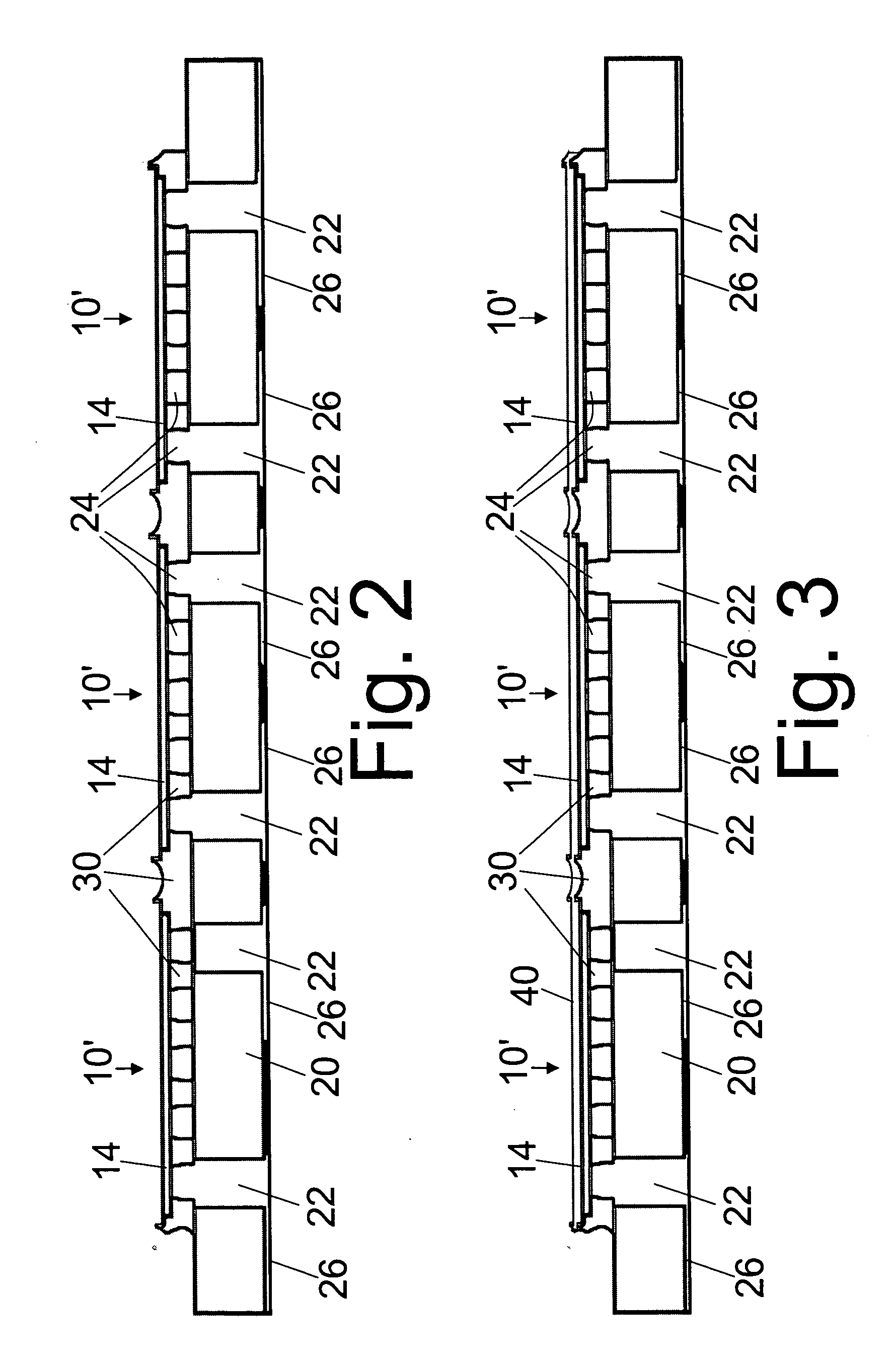
[0013] With reference to the FIGURES, an example fabrication process is set forth. Lateral flip chip LED chips 10 each including a substrate 12 and device layers 14 are bonded on a submount 20 with via connection 22 to the bottom of the submount 20 for electrical interconnection. In some embodiments, the light emitting diode chips 10 are group III nitride-based light emitting diode chips in which the device layers 14 are predominantly or entirely made up of layers of group III-nitride materials (such as GaN, AlN, InN, or binary or ternary alloys of these) and the substrate 12 is made of sapphire, SiC, GaN, or another suitable substrate for epitaxial growth of group III-nitride layers. The submount 20 is suitably made of an electrically insulating material such as alumina, semi-insulating silicon, BeO, AlN, or so forth, or of electrically insulating composites such as AlSiC, graphite-filled polymers, or so forth. Some suitable methods for forming the submount 20 with electrically con...


PUM


Abstract

A surface mount LED package having a tight footprint and small vertical image size is fabricated by a method comprising: forming light emitting diode chips each having a substrate and a plurality of layers configured to emit electroluminescence responsive to electrical energizing; forming electrical vias in a sub mount, the electrical vias passing from a front side of the sub-mount to a back-side of the sub-mount; flip chip bonding the light emitting diode chips on the front-side of the sub mount such that each light emitting diode chip electrically contacts selected electrical vias; thinning or removing the substrates of the flip-chip bonded light emitting diode chips; and after the thinning, disposing a phosphor over the flip chip bonded light emitting diode chips.

Description

[0001] This application claims the benefit of U.S. Provisional Application No. 60 / 731,078 filed Oct. 28, 2005. U.S. Provisional Application No. 60 / 731,078 is incorporated by reference herein in its entirety.BACKGROUND [0002] Tight footprint white light emitting diode (LED) packages usually include at least one conformal coating of phosphor applied on the LED chips. However, the vertical emission profile of the light source is limited by the height of the chip substrate. Also due to the side emission of the substrate, the phosphor is advantageously coated on the vertical sidewall to capture all the light. Phosphor coating on the sidewall can result in poor goniometric color uniformity due to phosphor thickness non-uniformity. Another disadvantage of a conformally coated small light source is heat-induced degradation of the host material for the phosphor layer, due to the fact that the phosphor blend is close to the chip and absorbs more radiometric power per unit area and in turn gen...

Claims


Application Information

Patent Timeline
IPC IPC(8): H01L21/00
CPCH01L25/0753H01L2933/0041H01L33/505H01L33/0079H01L2924/0002H01L33/0093H01L2924/00
Inventor GAO, XIANGSACKRISON, MICHAEL
Owner GE LIGHTING SOLUTIONS LLC
Why Eureka
Try Eureka