Nitride semiconductor light emitting device, method of manufacturing nitride semiconductor light emitting device, and nitride semiconductor transistor device

a technology of nitride semiconductor and light emitting device, which is applied in the direction of semiconductor lasers, solid-state devices, semiconductor lasers, etc., can solve the problems of many nitride semiconductor laser devices that stopped emitting laser light, and the cod of the light emitting portion was found to be a problem, so as to improve reliability, improve reliability, and improve reliability

Active Publication Date: 2007-09-06
SHARP FUKUYAMA LASER CO LTD
View PDF33 Cites 43 Cited by
  • Summary
  • Abstract
  • Description
  • Claims
  • Application Information

AI Technical Summary

Benefits of technology

[0009]Also in the case where a nitride semiconductor light emitting diode device is driven under the conditions of high temperature and high power, its light emitting surface that is the light emitting portion may be degraded, resulting in deteriorated reliability. Improved reliability is also desired in a nitride semiconductor transistor device such as HFET (Heterostructure Field Effec

Problems solved by technology

As a result, in the aging test under the conditions of low temperature and low power, the devices operated stably over 3000 hours.
In the aging test under the conditions of high temperature and high power, it was observed that many nitride semiconductor laser devices stopped emitting laser light after 400 hours or so, due to COD (Catastrophic Optical Damage) at the light emitting portion.
Therefore, in the conventional nitride semiconduc

Method used


Image

  • Nitride semiconductor light emitting device, method of manufacturing nitride semiconductor light emitting device, and nitride semiconductor transistor device
  • Nitride semiconductor light emitting device, method of manufacturing nitride semiconductor light emitting device, and nitride semiconductor transistor device
  • Nitride semiconductor light emitting device, method of manufacturing nitride semiconductor light emitting device, and nitride semiconductor transistor device

Examples


first embodiment

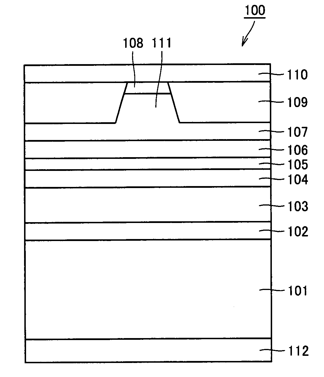
[0053]FIG. 1 is a cross section schematically showing a preferable example of a nitride semiconductor laser device in the present embodiment. Here, a nitride semiconductor laser device 100 in the present embodiment is configured to include a buffer layer 102 having a thickness of 0.2 μm made of n-type GaN, an n-type cladding layer 103 having a thickness of 2.3 cm made of n-type Al0.06Ga0.94N, an n-type guide layer 104 having a thickness of 0.02 μm made of n-type GaN, a multiple quantum well active layer 105 made of 4 nm-thick InGaN and 8 nm-thick GaN, a p-type current block layer 106 having a thickness of 20 nm made of p-type Al0.3Ga0.7N, a p-type cladding layer 107 having a thickness of 0.5 cm made of p-type Al0.05Ga0.95N, and a p-type contact layer 108 having a thickness of 0.1 μm made of p-type GaN, which are stacked on a semiconductor substrate 101 made of n-type GaN in this order from semiconductor substrate 101 by epitaxial growth. Here, the mixed crystal ratio in each of the ...

second embodiment

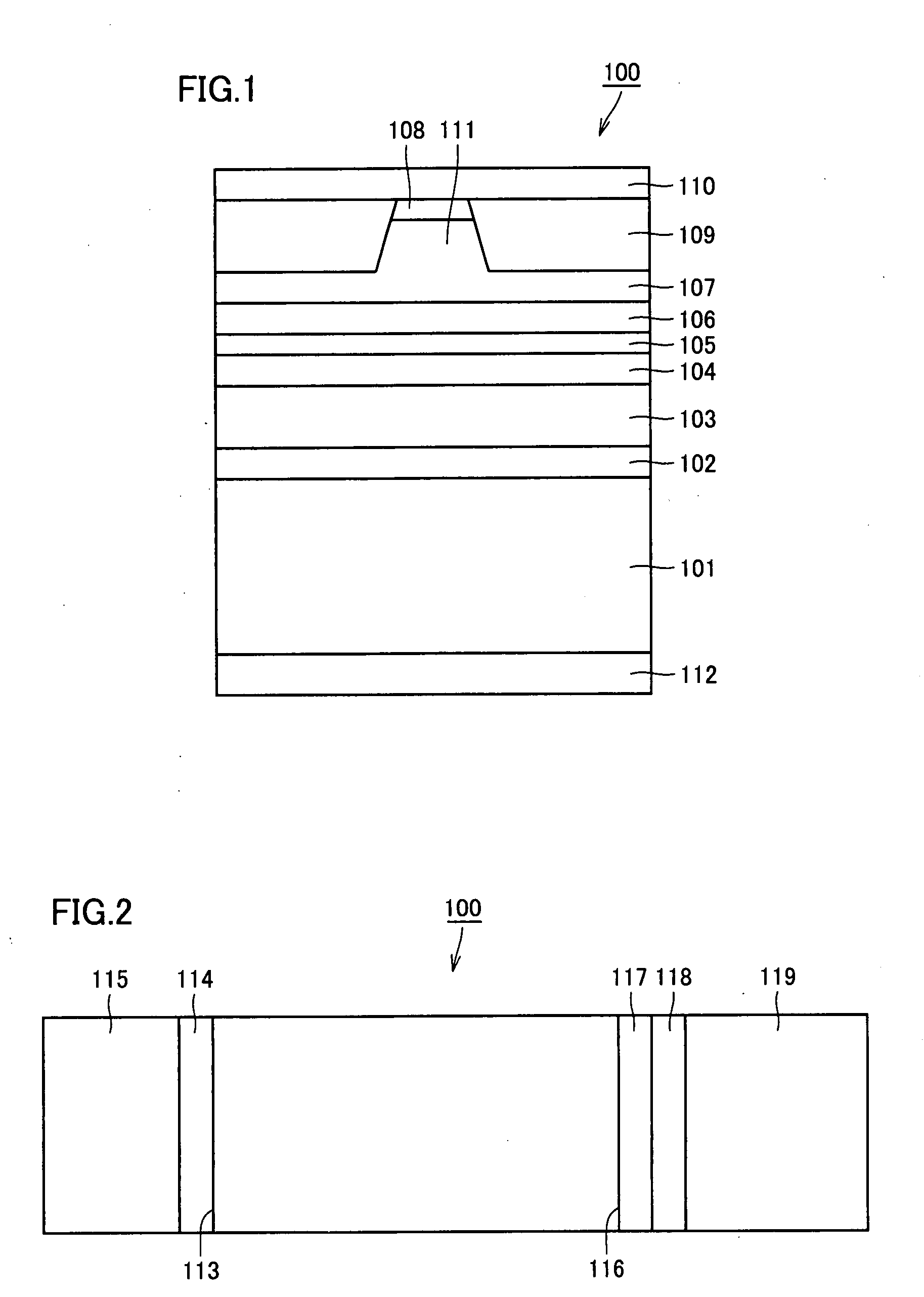
[0084]A nitride semiconductor laser device in the present embodiment has the similar configuration as that of the nitride semiconductor laser device in the first embodiment, except that a configuration of a film formed on facet 113 at the light emitting side and a configuration of a film formed on facet 116 at the light reflecting side are changed.

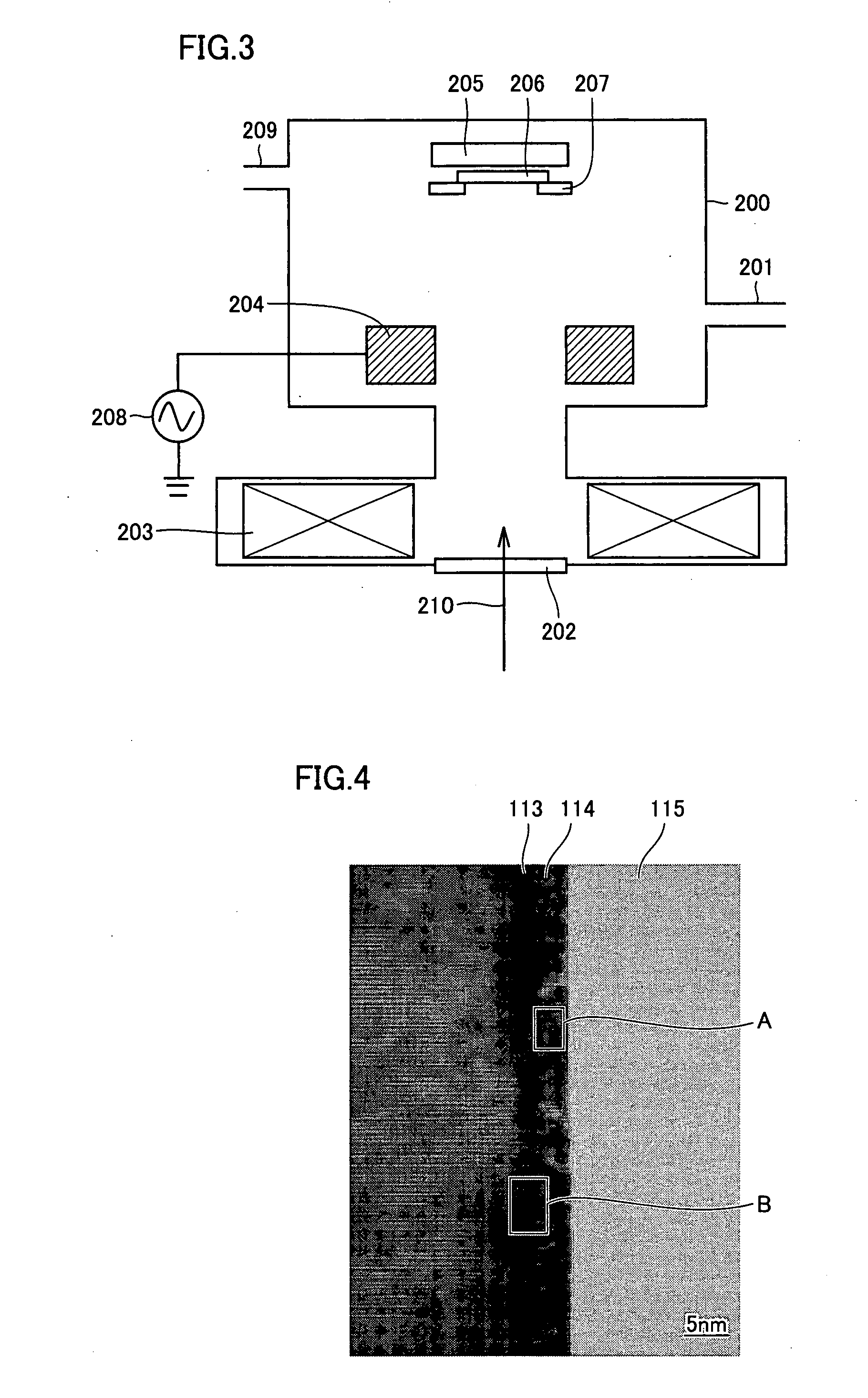
[0085]In the nitride semiconductor laser device in the present embodiment, coat film 114 having a thickness of 20 nm made of aluminum nitride is formed on facet 113 at the light emitting side, and aluminum oxide film 115 having a thickness of 200 nm is formed on coat film 114.

[0086]An aluminum nitride film having a thickness of 12 nm is formed on facet 116 at the light reflecting side, an aluminum oxide film having a thickness of 80 nm is formed on the aluminum nitride film, and a high reflection film is formed on the aluminum oxide film by stacking four pairs of a silicon oxide film having a thickness of 81 nm and a titanium oxide film ha...

third embodiment

[0089]A nitride semiconductor laser device in the present embodiment has the similar configuration as that of the nitride semiconductor laser device in the first embodiment, except that a configuration of a film formed on facet 113 at the light emitting side and a configuration of a film formed on facet 116 at the light reflecting side are changed.

[0090]In the nitride semiconductor laser device in the present embodiment, coat film 114 having a thickness of 40 nm made of aluminum oxynitride represented by a composition formula Al0.33O0.11N0.56 is formed on facet 113 at the light emitting side, and aluminum oxide film 115 having a thickness of 240 nm is formed on coat film 114.

[0091]An aluminum nitride film having a thickness of 12 nm is formed on facet 116 at the light reflecting side, an aluminum oxide film having a thickness of 80 nm is formed on the aluminum nitride film, and a high reflection film is formed on the aluminum oxide film by stacking four pairs of a silicon oxide film...


PUM


Abstract

Provided are a nitride semiconductor light emitting device including a coat film formed at a light emitting portion and including an aluminum nitride crystal or an aluminum oxynitride crystal, and a method of manufacturing the nitride semiconductor light emitting device. Also provided is a nitride semiconductor transistor device including a nitride semiconductor layer and a gate insulating film which is in contact with the nitride semiconductor layer and includes an aluminium nitride crystal or an aluminum oxynitride crystal.

Description

[0001]This nonprovisional application is based on Japanese Patent Applications Nos. 2006-059695 and 2007-009282 filed with the Japan Patent Office on Mar. 6, 2006 and Jan. 18, 2007, the entire contents of which are hereby incorporated by reference.BACKGROUND OF THE INVENTION[0002]1. Field of the Invention[0003]The present invention relates to a nitride semiconductor light emitting device, a method of manufacturing a nitride semiconductor light emitting device, and a nitride semiconductor transistor device.[0004]2. Description of the Background Art[0005]Generally, among nitride semiconductor light emitting devices, nitride semiconductor laser devices are known for low reliability caused by degradation of light emitting portions. The degradation of a light emitting portion is considered to be caused by excessively generated heat from the light emitting portion due to the presence of a non-radiative recombination level. Oxidation of the light emitting portion is thought to be the main ...

Claims


Application Information

Patent Timeline
IPC IPC(8): H01L33/00H01L21/336H01L21/338H01L29/778H01L29/78H01L29/812H01S5/028H01S5/343
CPCB82Y20/00H01L29/2003H01L29/7786H01S5/34333H01L33/44H01S5/028H01S5/22H01L29/7787
Inventor KAMIKAWA, TAKESHIKAWAGUCHI, YOSHINOBU
Owner SHARP FUKUYAMA LASER CO LTD
Why Eureka
Try Eureka