Sheet-Like Probe, Method Of Producing The Probe, And Application Of The Probe

a probe and sheet-like technology, applied in the field of sheet-like probes, can solve the problems of difficult to cause each inspection electrode of the probe, difficult to manufacture the probe for inspection itself, and high cost of the probe for inspection, etc., to achieve easy connection of the electrode structure, high durability, and large thickness of the electrode structur

Active Publication Date: 2007-09-06
ISC CO LTD
View PDF3 Cites 14 Cited by
  • Summary
  • Abstract
  • Description
  • Claims
  • Application Information

AI Technical Summary

Benefits of technology

[0148] According to the sheet-like probe in accordance with the present invention, a diameter of the base end of the surface electrode portion of the electrode structure is larger than a diameter of the end of the side which comes into contact with the surface electrode portion on the short circuit portion. Even in the case in which the surface electrode portion has a small diameter, therefore, the electrode structure can be prevented from slipping from the insulating layer so that a high durability can be obtained.
[0149] According to the sheet-like probe in accordance with the present invention, a thickness of the electrode structure is large. Even in the case in which the periphery of an electrode to be inspected in a circuit device to be inspected is covered by an insulating layer having a large thickness, therefore, it is easy to connect the electrode structure and the electrode to be inspected.
[0150] According to the sheet-like probe in accordance with the present invention, even in the case in which an inspecting object is a wafer having a large area in a diameter of 8 inches or more and a circuit device having a very small pitch of the electrode to be inspected of 120 μm or less, a tip of the surface electrode portion has a suitable diameter and a projection height is large, and a diameter of the surface electrode portion is larger than a diameter of the short circuit portion, an insulating property between adjacent electrode structures can be ensured and the electrode structure can be prevented from slipping from the insulating layer. In addition, since a thickness of the insulating layer is small, it is easy to move the electrode structure in a direction of a thickness, and a concave and convex absorbing ability of the sheet-like probe is increased.
[0151] Consequently, a concave and convex absorbing ability of the probe card using the sheet-like probe in accordance with the present invention is improved. Moreover, even in the case in which an electrode to be inspected in a circuit device to be inspected has a variation in height, an electrical connection of the probe card to each electrode to be inspected can be easily achieved.
[0152] According to the sheet-like probe in accordance with the present invention, the short circuit portion of the electrode structure can be moved in a direction of a thickness of the insulating layer, thereby increasing a concave and convex absorbing ability of the sheet-like probe.
[0153] Consequently, a concave and convex absorbing ability of the probe card using the sheet-like probe in accordance with the present invention is improved. Moreover, even in the case in which an electrode to be inspected in a circuit device to be inspected has a variation in height, an electrical connection of the probe card to each electrode to be inspected can be easily achieved.

Problems solved by technology

However, in the case in which the circuit to be inspected is a wafer having a large number of integrated circuits formed thereon, it is necessary to arrange a large number of inspection electrodes when fabricating a probe for an inspection to inspect the wafer.
Therefore, the probe for an inspection is very expensive.
Moreover, in the case in which the pitch of the electrodes to be inspected is small, it is hard to carry out the fabrication of the probe for an inspection itself.
For this reason, it is practically hard to cause each of the inspection electrodes of the probe for an inspection to come in contact with a large number of electrodes to be inspected in the wafer stably and reliably.
However, the probe for an inspection has the following problems.
For this reason, it is hard to achieve a stable electrical connection to the circuit device to be inspected.
In the electrolytic plating treatment, moreover, it is actually difficult to supply a current having an even current density distribution to the whole surface of the metal layer 92.
In a sheet-like probe obtained by the former means, however, it is hard to reliably achieve a stable electrical connection to the electrode to be inspected.
Consequently, it is hard to actually use the sheet-like probe.
Accordingly, there is a case in which it is difficult to form the surface electrode portion having a large projection height.
In the case in which a thickness of the electrode structure of the sheet-like probe is decreased and, for instance, the periphery of an electrode to be inspected in a circuit device to be inspected is covered by an insulating layer having a large thickness, it may be difficult to connect the electrode structure and the electrode to be inspected.
Accordingly, since there is increased a compressive deformation amount of a conductive portion in an anisotropically conductive connector, a permanent deformation of a conductive portion in an anisotropically conductive connector occurs early and an electrical connection is made difficult, thereby requiring an exchange of the anisotropically conductive connector and increasing an inspection cost.
In addition, in the case in which an electrode to be inspected in a circuit device is a solder bump electrode having a large variation in height, it may be impossible to achieve an electrical connection of the probe card to each electrode to be inspected.
However, the above described anisotropically conductive connector has a following problem in practice.
Consequently, it is extremely hard to actually use the complex conductive sheet individually.
As a result, there are problems in the case in which a sheet-like connector is used as a sheet-like probe for inspecting a wafer.
However, in the case in which a diameter φ1 of an opening is made larger while a disposition pitch of an electrode structure is kept constant, an insulating property between adjacent electrode structures cannot be ensured.
As a result, there is a problem that a variation of electric resistance values between electrode structures formed in the sheet-like probe may become larger.

Method used


Image

  • Sheet-Like Probe, Method Of Producing The Probe, And Application Of The Probe
  • Sheet-Like Probe, Method Of Producing The Probe, And Application Of The Probe
  • Sheet-Like Probe, Method Of Producing The Probe, And Application Of The Probe

Examples


first embodiment

Sheet-Like Probe of the First Embodiment

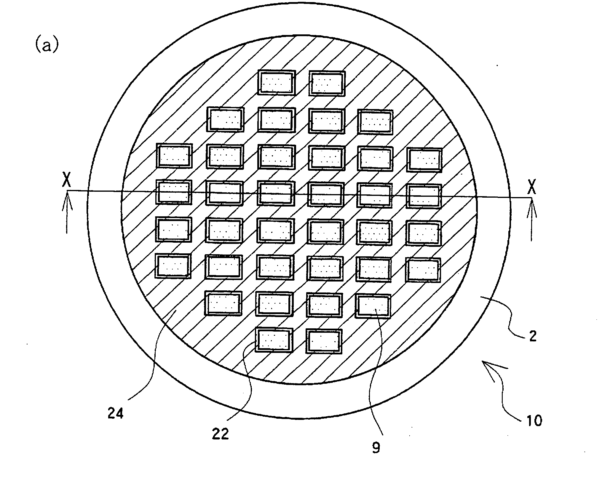
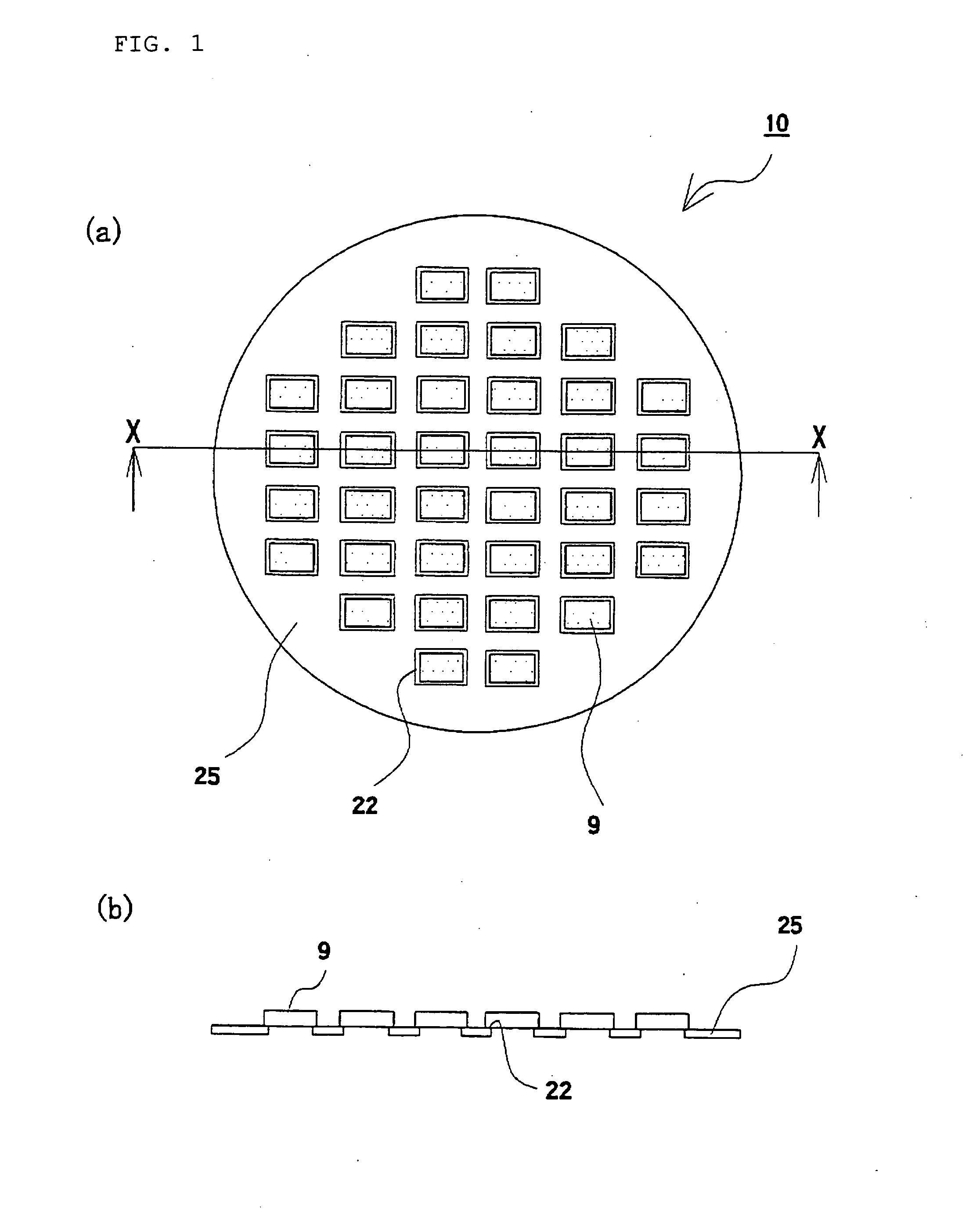
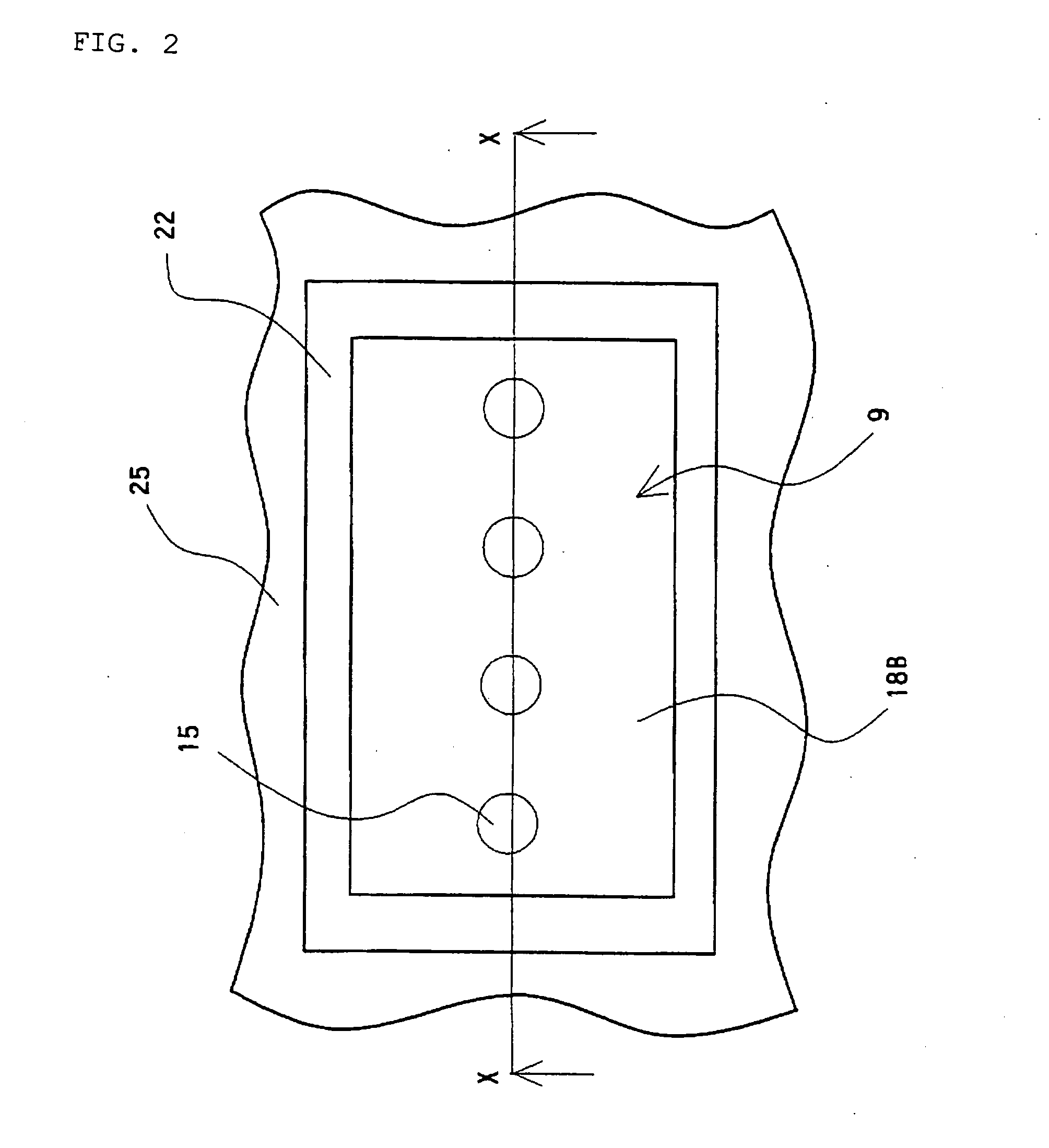
[0308]FIG. 1 is an explanatory sectional view showing a structure of a first embodiment of a sheet-like probe according to the present invention, FIG. 1(a) being a plan view and FIG. 1(b) being a sectional view taken along an X-X line, FIG. 2 is a plan view showing an enlarged contact film in the sheet-like probe of FIG. 1, FIG. 3 is an explanatory sectional view showing a structure of the sheet-like probe according to the present invention, and FIG. 4 is an explanatory sectional view showing an enlarged electrode structure in the sheet-like probe according to the present invention.

[0309] A sheet-like probe 10 according to the present embodiment is used for carrying out an electrical inspection for each integrated circuit in a state of a wafer for a wafer having a size of 8 inches or the like in which a plurality of integrated circuits is formed.

[0310] As shown in FIG. 1(a), the sheet-like probe 10 has a metal flame plate 25 having a through...

second embodiment

Sheet-Like Probe of the Second Embodiment

[0444] The sheet-like probe 10 of a second embodiment according to of the present invention will be described below in detail.

[0445]FIG. 7 is an explanatory sectional view showing a structure of a sheet-like probe related to a second embodiment according to the present invention, and FIG. 8 is an explanatory sectional view showing an enlarged electrode structure in the sheet-like probe related to a second embodiment according to the present invention.

[0446] As shown in FIG. 7, each of the electrode structures 15 is provided with a projected surface electrode portion 16 which is exposed from a surface of the insulating layer 18B and projected from the surface of the insulating layer 18B. The electrode structure 15 is also provided with a rectangular plate-shaped back electrode portion 17 exposed from a back face of the insulating layer 18B. The electrode structure 15 is also provided with a short circuit portion 18 extended to penetrate in t...

example 1

[0554] There was prepared a laminated polyimide sheet in which a metal layer formed of copper having a diameter of 20 cm and a thickness of 4 μm is laminated on both sides of a polyimide sheet having a diameter of 20 cm and a thickness of 12.5 μm (which will be hereinafter referred to as “a laminate material 10A” (see FIG. 14(a)).

[0555] The laminate material 10A has a first back side metal layer 19A formed of copper having a thickness of 4 μm on one of surfaces of an insulating sheet 11 formed by a polyimide sheet having a thickness of 12.5 μm and has a surface side metal layer 16A formed of copper having a thickness of 4 μm on the other surface.

[0556] For the laminate material 10A, a protective film 40A was formed over a whole surface of the surface side metal layer 16A through a protective seal formed of polyethylene terephthalate having a thickness of 25 μm. Furthermore, a resist film 12A provided with 26116 circular pattern holes 12H having a diameter of 45 μm was formed on a ...


PUM

PropertyMeasurementUnit
thicknessaaaaaaaaaa
angleaaaaaaaaaa
diameteraaaaaaaaaa

Abstract

A sheet-like probe and a method of producing the probe. In the probe electrode structure bodies do not come out from an insulation film and achieve high durability, and in a burn-in test for a wafer having a large area and for a circuit device having to-be-inspected electrodes with small intervals, positional displacement, caused by temperature variation, between the electrode structure bodies and the to-be-inspected electrode can be reliably prevented for stable connection conditions. The sheet-like probe includes an insulation layer and a contact film provided with electrode structure bodies arranged on the insulation layer to be apart from each other in the surface direction of the insulation layer and penetratingly extend in the thickness direction of the insulation layer. The electrode structure bodies each are composed of a surface electrode section exposed to the front surface of the insulation layer.

Description

TECHNICAL FIELD [0001] The present invention relates to a sheet-like probe which is suitable for a probe apparatus to carry out an electrical connection to a circuit, a method of manufacturing the probe and an application thereof in an electrical inspection for a circuit such as an integrated circuit. BACKGROUND ART [0002] For example, in an electrical inspection for a wafer on which a large number of integrated circuits are formed or a circuit device such as an electronic component, for example, a semiconductor device, there has been used a probe for an inspection which has inspection electrodes arranged in accordance with a pattern corresponding to a pattern of electrodes to be inspected in a circuit device to be inspected. [0003] Conventionally, there has been used a probe for an inspection in which the inspection electrodes formed by a pin or a blade are arranged. [0004] However, in the case in which the circuit to be inspected is a wafer having a large number of integrated circ...

Claims


Application Information

Patent Timeline
Patent Type & Authority Applications(United States)
IPC IPC(8): G01R31/02A63H17/045A63H31/08A63H29/22A63H30/00A63H30/04A63H31/00B60K17/16F16H1/14F16H1/20F16H1/28F16H48/08G01R1/06G01R1/067G01R1/073G01R3/00G01R31/26H01L21/06H01L21/66H01L51/50H05B33/14
CPCA63H29/22A63H30/04A63H31/00F16H48/08Y10T29/49155G01R1/0735G01R3/00H01L51/5012H05B33/14G01R1/06711H10K50/11H01L22/00G01R1/06G01R1/073
Inventor SATO, KATSUMIINOUE, KAZUOFUJIYAMA, HITOSHIYOSHIOKA, MUTSUHIKOIGARASHI, HISAO
Owner ISC CO LTD
Why Eureka
Try Eureka