

Device for final inspection
a technology for semiconductor components and devices, applied in measurement devices, electrical testing, instruments, etc., can solve the problem that no oxide can form on the metal surface of contact pins, and achieve the effect of improving the service life of contact pins and improving the measurement reliability of test devices
- Summary
- Abstract
- Description
- Claims
- Application Information
AI Technical Summary
Benefits of technology
Problems solved by technology
Method used
Image

Examples
Embodiment Construction
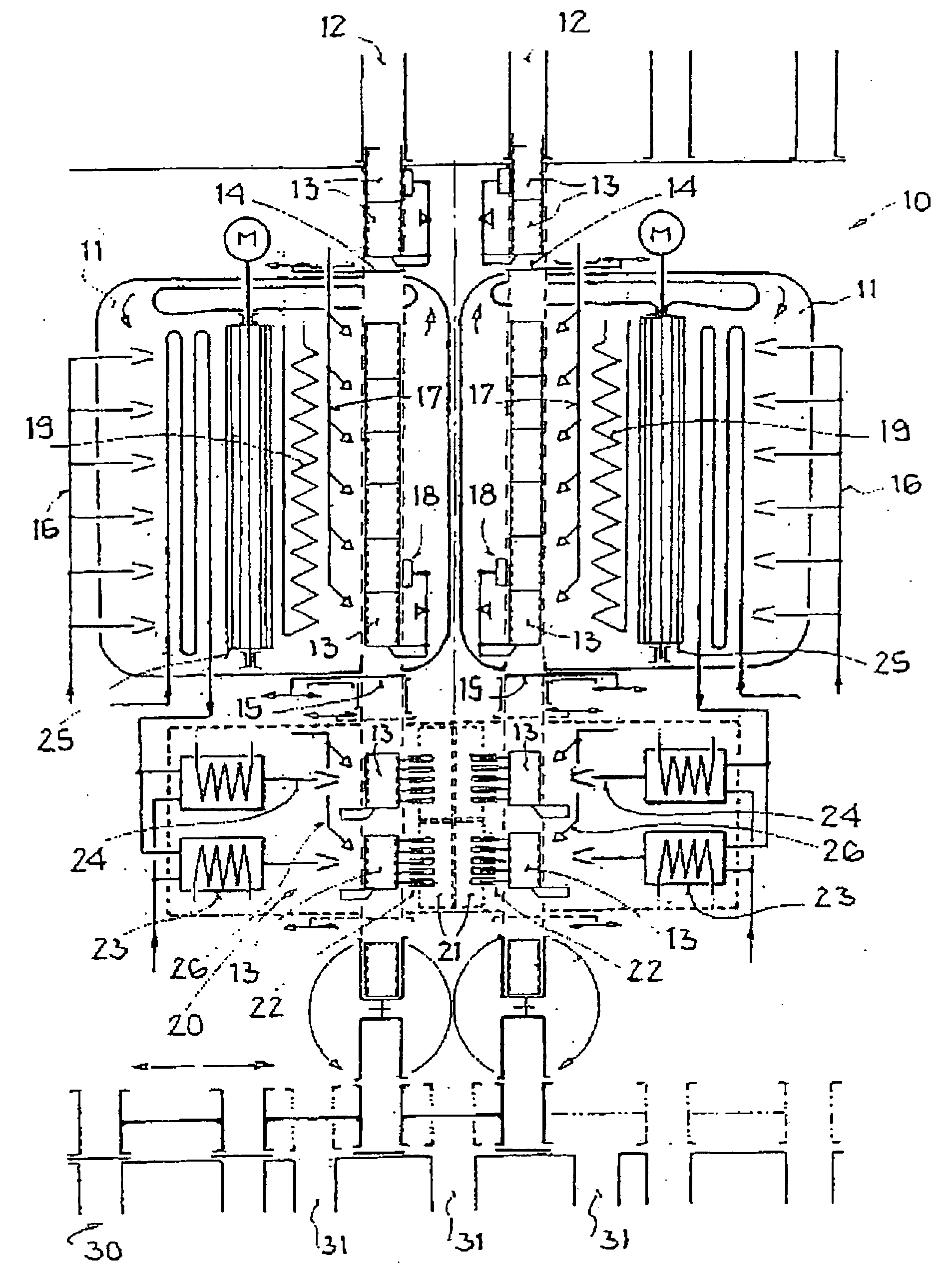
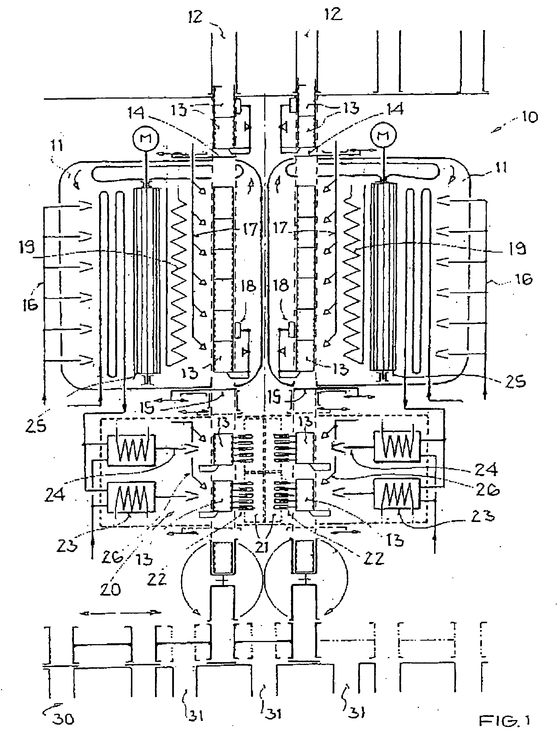
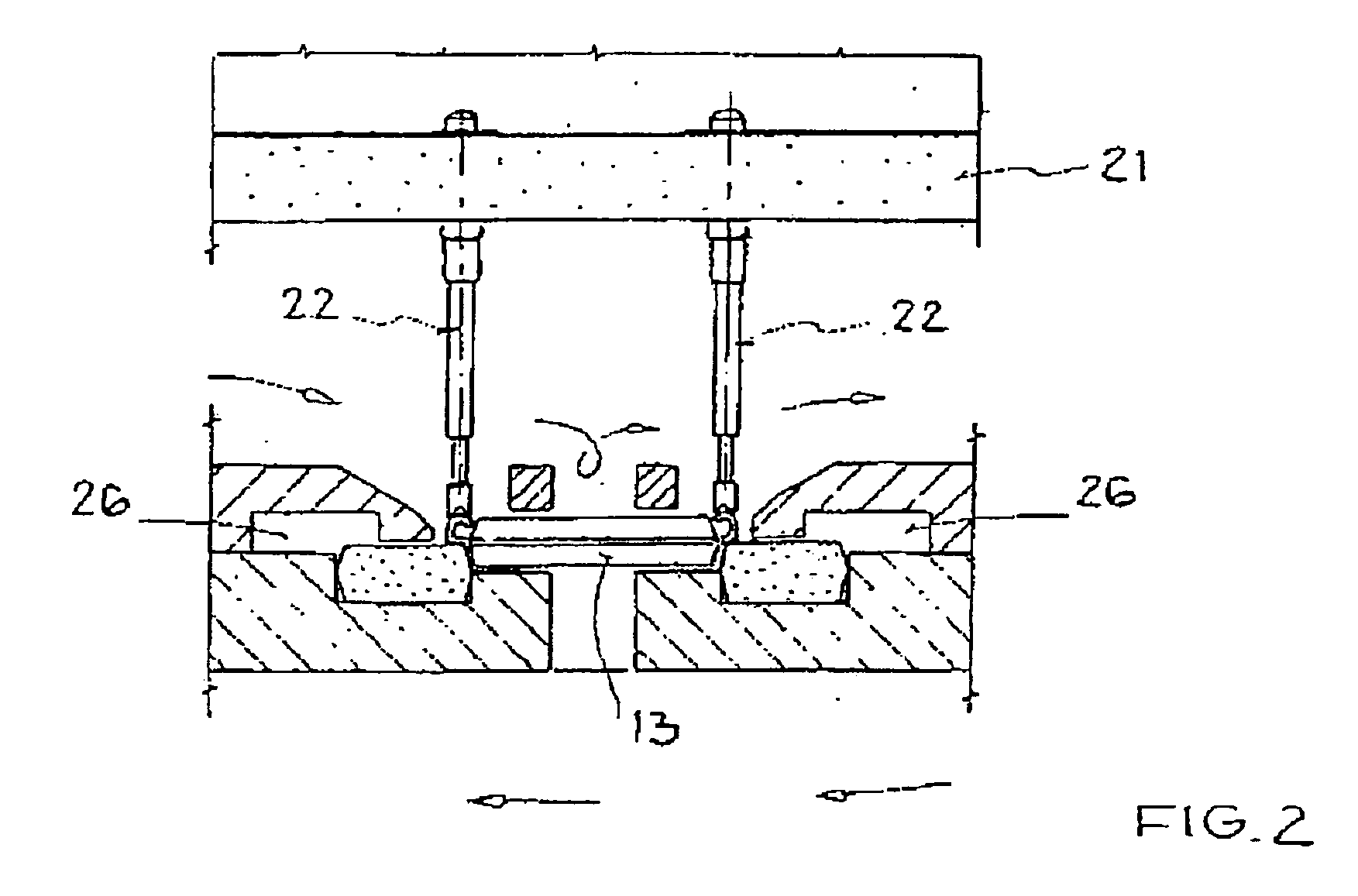
[0034]FIG. 1 shows an environmental chamber 10 of a handler with a left-hand and a right-hand holding chamber 11. Singulated ICs 13 are supplied to the environmental chamber 10 through loading devices 12. The holding chambers 11 are each closed off from the open areas of the handler by a chamber entry closure 14 and a chamber exit closure 15 in order to heat or cool the ICs 13 for testing to a defined test temperature.
[0035]Three temperature ranges are distinguished. During testing at low temperatures, which takes place at approximately −40° C., liquid nitrogen is supplied to the holding chambers 11 through separate lines and nozzles 16. Normally, temperature regulation of the ICs 13 is accomplished under program control, so no influences can act on the atmosphere inside the environmental chamber 10. Transport of the ICs 13 inside the environmental chamber 10 takes place by means of a pneumatically controlled device with lines and nozzles 17. In addition, holding devices 18 are loca...
PUM
 Abstract
Description
Claims
Application Information