Via transmission lines for multilayer printed circuit boards

a technology of printed circuit board and transmission line, which is applied in the direction of printed element electric connection formation, inspection/indentification of circuits, waveguide type devices, etc., can solve the problems of worse electrical performance of whole interconnect circuits, and achieve high performance

Active Publication Date: 2007-09-06
RENESAS ELECTRONICS CORP +1
View PDF16 Cites 54 Cited by
  • Summary
  • Abstract
  • Description
  • Claims
  • Application Information

AI Technical Summary

Benefits of technology

[0004] Accordingly, they are primary objects of the present invention to provide the high performance in the wide frequency band of a via transition consisting of a signal via or a number of signal vias surrounded by ground vias and shielding properties of the via transition in a multilayer PCB.

Problems solved by technology

However, transitions providing connections between different signal layers of the multilayer PCB by means of via structures have usually high enough return and leakage losses that finally make worse the electrical performance of whole interconnect circuits embedded in the multilayer PCB.

Method used


Image

  • Via transmission lines for multilayer printed circuit boards
  • Via transmission lines for multilayer printed circuit boards
  • Via transmission lines for multilayer printed circuit boards

Examples


Embodiment Construction

[0031] The following description of the preferred embodiments directed to a single via transmission line mainly but it, is well understood that it is not limited to such an application and can be used to any number of via transmission lines in a multilayer PCB, including that forming complex high-density via configurations, and also these via transmission lines can be jointed to any types of interconnect circuits including planar transmission lines embedded in the multilayer PCB, coaxial cables, pins from Large-Scale Integration (LSI) chip packages, and so on.

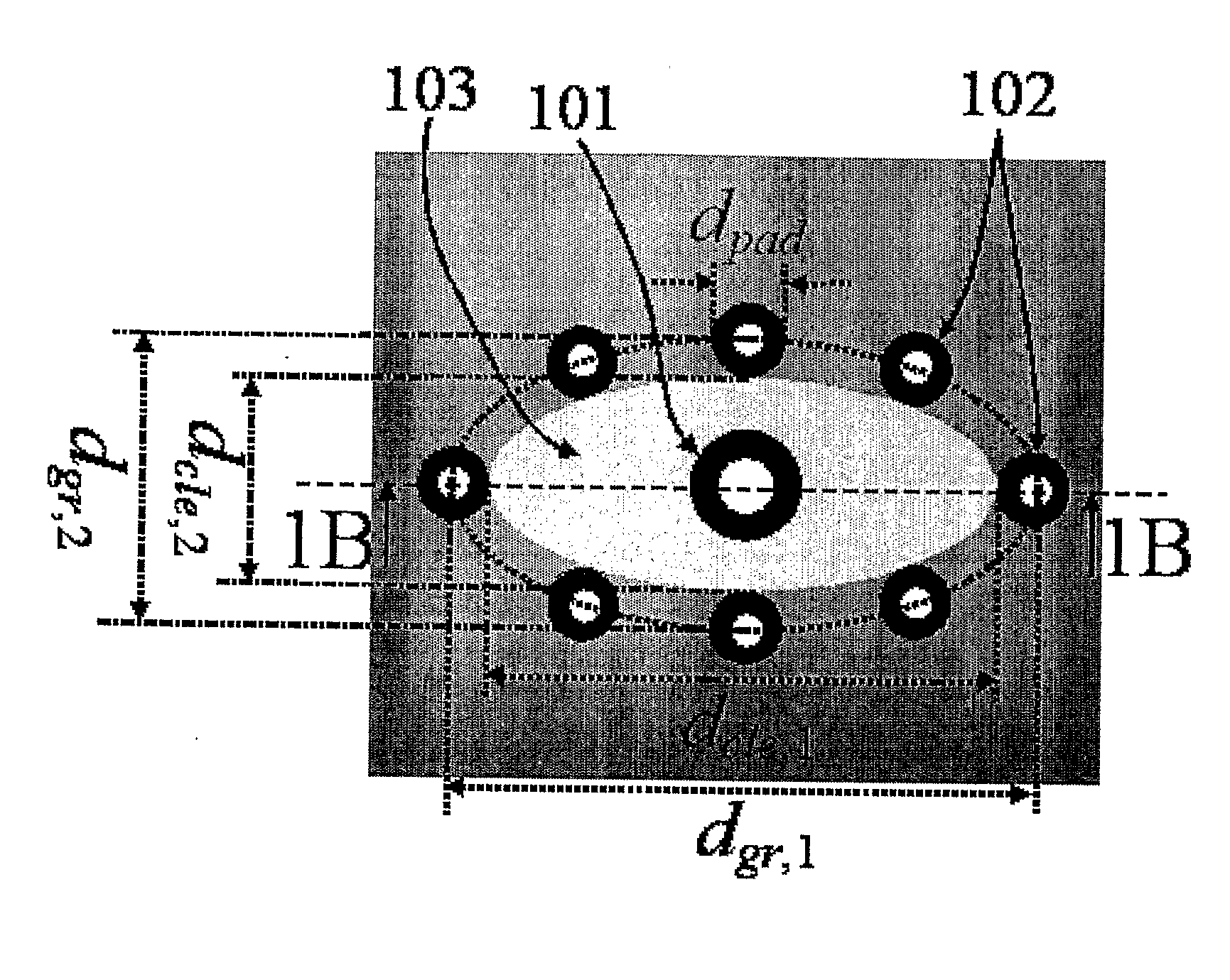
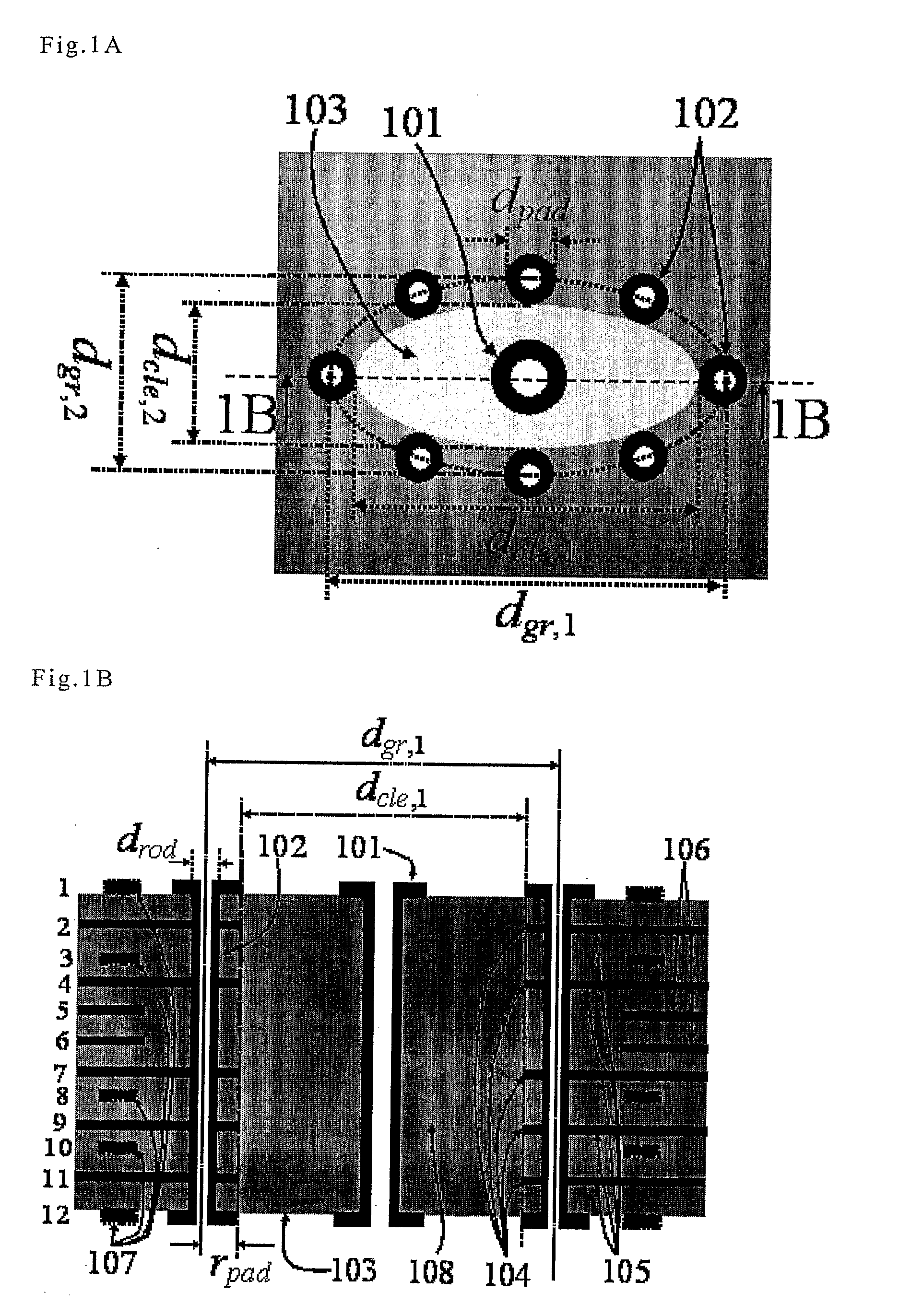
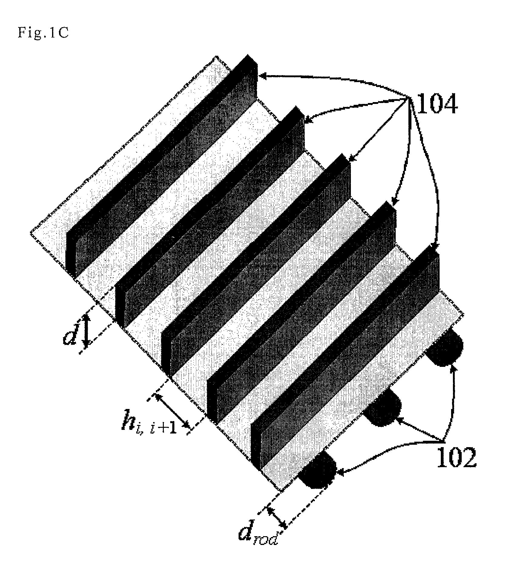
[0032] Referring to the drawings, a via transmission line in a 12-conductor-layer PCB, which serves only as an example of multilayer PCB design consisting of ground planes 105, power supplying planes 106, signal layers 107, and isolating material 108, is shown in FIGS. 1A and 1B (numbering of conductive layers is demonstrated in FIG. 1B). The via transmission line consists of a signal via 101 (central conductor) forming an inn...


PUM


Abstract

A via transmission line for a multilayer printed circuit board (PCB) in which a wave guiding channel is formed by a signal via or a number of signal vias, an assembly of ground vias surrounding the signal via or corresponding number of coupled signal vias, a set of ground plates from conductor layers of the multilayer PCB, and a clearance hole. In this via transmission line, the signal via, or the number of signal vias forms an inner conductive boundary, ground vias and ground plates from conductor layers of the multilayer PCB form an outer conductive boundary, and the clearance hole provides both isolation of the inner conductive boundary from the outer conductive boundary and high-performance broadband operation of the via transmission line by means of the predetermined clearance hole cross-sectional shape and dimensions where the cross-sectional shape of the clearance hole is defined by the arrangement of ground vias in the outer conductive boundary and dimensions of the clearance hole are determined according to a method to minimize frequency-dependent return losses caused by specific corrugations of the outer conductive boundary formed by ground plates in the wave guiding channel of the via transmission line.

Description

TECHNICAL FIELD [0001] This invention relates to transitions between planar layers of a multilayer printed circuit board (PCB) which are formed as broadband shielded via transmission lines which is formed by a signal via or a number of coupled signal vias as an inner conductive boundary, ground vias and ground layers from conductor layers of the multilayer PCB as an outer conductive boundary, and a clearance hole isolating the inner and outer conductive boundary of the via transmission line. The broadband operation of the transmission line is achieved by means of predetermined form and dimensions of the clearance hole. Shielded properties of the transmission line are provided by the outer boundary of the via transmission line formed by the ground vias and the ground plates. The characteristic impedance control is carried out by a determination of appropriate dimensions of inner and outer conductive boundaries of the via transmission line proceeding from a formula for corresponding c...

Claims


Application Information

Patent Timeline
Patent Type & Authority Applications(United States)
IPC IPC(8): H01P5/02H05K1/02H05K3/42H05K3/46
CPCH05K1/0222H05K1/0269H05K3/429H05K2201/09809H05K2201/09618H05K2201/09718H05K2201/09536
Inventor KUSHTA, TARASNARITA, KAORUTOHYA, HIROKAZUSAEKI, TAKANORIKANEKO, TOMOYUKI
Owner RENESAS ELECTRONICS CORP
Why Eureka
Try Eureka