
Transfer of wafers with edge grip

a technology of transfer and edge grip, which is applied in the direction of transportation and packaging, coating, layered products, etc., can solve the problems of economic disadvantage, expected operation, and difficulty in wafer support and handling

Inactive Publication Date: 2007-09-20
APPLIED MATERIALS INC
View PDF21 Cites 26 Cited by
  • Summary
  • Abstract
  • Description
  • Claims
  • Application Information

AI Technical Summary

Benefits of technology

[0013] One embodiment of the present invention includes an apparatus for transferring a wafer during thermal processing. The wafer handling apparatus comprises a loading blade for delivering the wafer into the heating chamber and at least three wafer handlers for transferring the wafer between the loading blade and an edge ring in an inverted orientation. At least two wafer handlers are edge handlers for supporting the wafer at two opposite wafer edges thereof within a distance that is less than the wafer edge exclusion zone, and one of the two edge handlers is configured to restrain the wafer from lateral movement, while another edge handler is configured to adapt to the thermal expansion of the wafer. The third handler is configured to gravitationally support the wafer in a horizontal position independently from the co-planar edge handlers. The three handlers transfer the wafer without movement of the loading blade.
[0014] Another embodiment of the present invention includes a wafer lifting apparatus. The apparatus comprises a drive and an arm connected to the drive. Three effectors are coupled to the arm and adapted to gravitationally support a wafer in an invert orientation during transfer. Two effectors are co-planar with the front surface of the wafer and support the wafer in a horizontal position at two opposite edges within a distance that is less than the wafer exclusion zone, preferably, less than 1.5 mm. In one embodiment, one of the two edge or end effectors is configured to restrain the wafer from lateral movement, and another is configured to compensate for the thermal horizontal expansion of the wafer. The third effector supports the wafer from a back side independently from the two end effectors by chucking the wafer for example, with a vacuum. The back effector and the arm comprise a vacuum passage connected to the vacuum source.
[0015] The three effectors may be manipulated within the heating chamber through vacuum tight sealed apertures, with the arm positioned outside of the heating chamber. The sealed aperture may include a two-dimensionally flexible bellows. Alternatively, the arm may be manipulated the within the heating chamber through a vacuum tight sealed aperture. The sealed aperture can be configured to flexibly compensate for the movement of the end effectors and the back effector, or, alternatively, of the arm. A controller may be connected to the drive and the vacuum source to independently control the end effectors, the back effector and the arm. The three effectors and the arm may be made out of quartz.
[0016] A method of the present invention may include loading and unloading a wafer into and out of a heating chamber for thermal processing in which a wafer is delivered on a loading blade with a front side facing downwardly. Two effectors are moved to support the wafer in a horizontal inverted orientation at opposite edges within less than 1.5 mm contact, to restrain it from lateral movement, and to compensate for the thermal expansion of the wafer. The loading blade is retracted, and the effectors are lowered to the position of pre-heat. After the pre-heat, the wafer is loaded on an edge ring for thermal processing, and the end effectors are retracted. A back effecter then is lowered to grip the wafer at a back side, by chucking, and to unload it from the edge ring. Next, the back effector is moved to position the wafer for being placed over the two end effectors that are moved to receive and support the wafer. The back effector is retracted, and the loading blade is extended to receive the wafer and remove it from the chamber as the loading blade is retracted.

Problems solved by technology

Dies may be formed within the exclusion zone, but they usually have less than the full rectangular area and in any case are not expected to be operative.
However, using an inverted wafer orientation in the RTP reactor for the most part designed for conventional upwardly facing orientation presents some difficulties with wafer support and handling.
However, this solution has disadvantages.
Secondly, different integrated circuit designs likely have different die sizes and ratio of length to width.
Although feasible, this design is economically disadvantageous.
A problem with this solution is that the support may not be sufficiently reliable to avoid light leakage around the edge ring 14 as it provides only minimal overlap to the wafer 12 in the areas of the cut-outs 62.
However, even if all these requirements were met, this arrangement presents still another problem because the pins 43 would support the wafer so close to the wafer edge that the wafer will be unstable.
Still another problem is that, since the 300 mm wafers are so large, a wafer may bow, or sag, in the middle, between the supporting pins.
Finally, for this arrangement, the inverted orientation of the wafer would require a more sophisticated, and therefore more expensive, loading blade assembly to move the wafer into and out of the RTP reactor.
Substantial redesigning of the edge ring and loading blade to cooperate with the lift pins 43 is undesirable due to the expense and time that would be required.

Method used


Image

  • Transfer of wafers with edge grip
  • Transfer of wafers with edge grip
  • Transfer of wafers with edge grip

Examples


Embodiment Construction

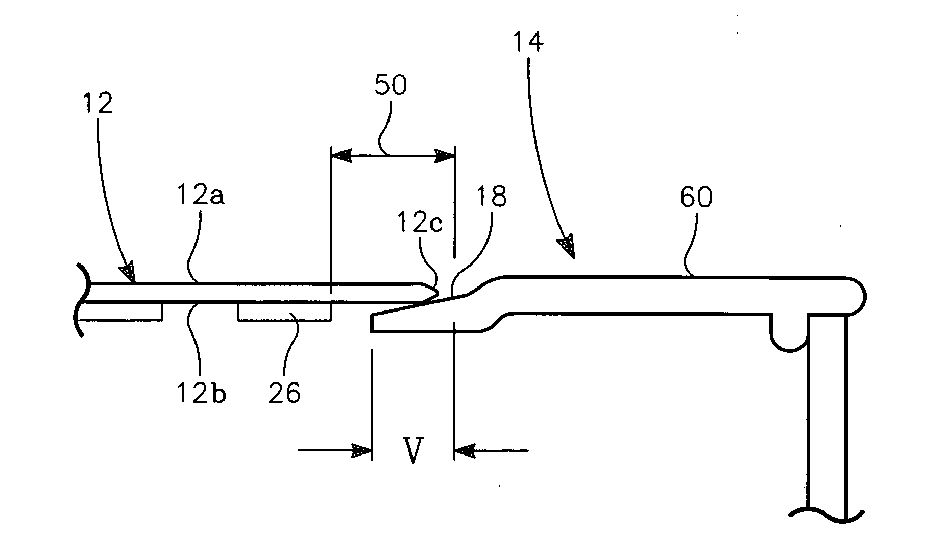
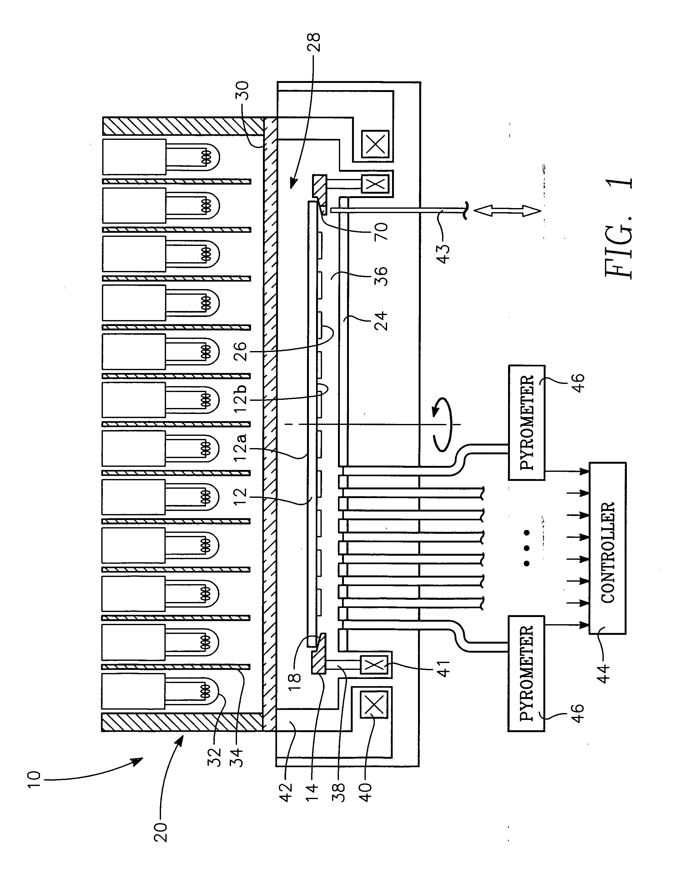
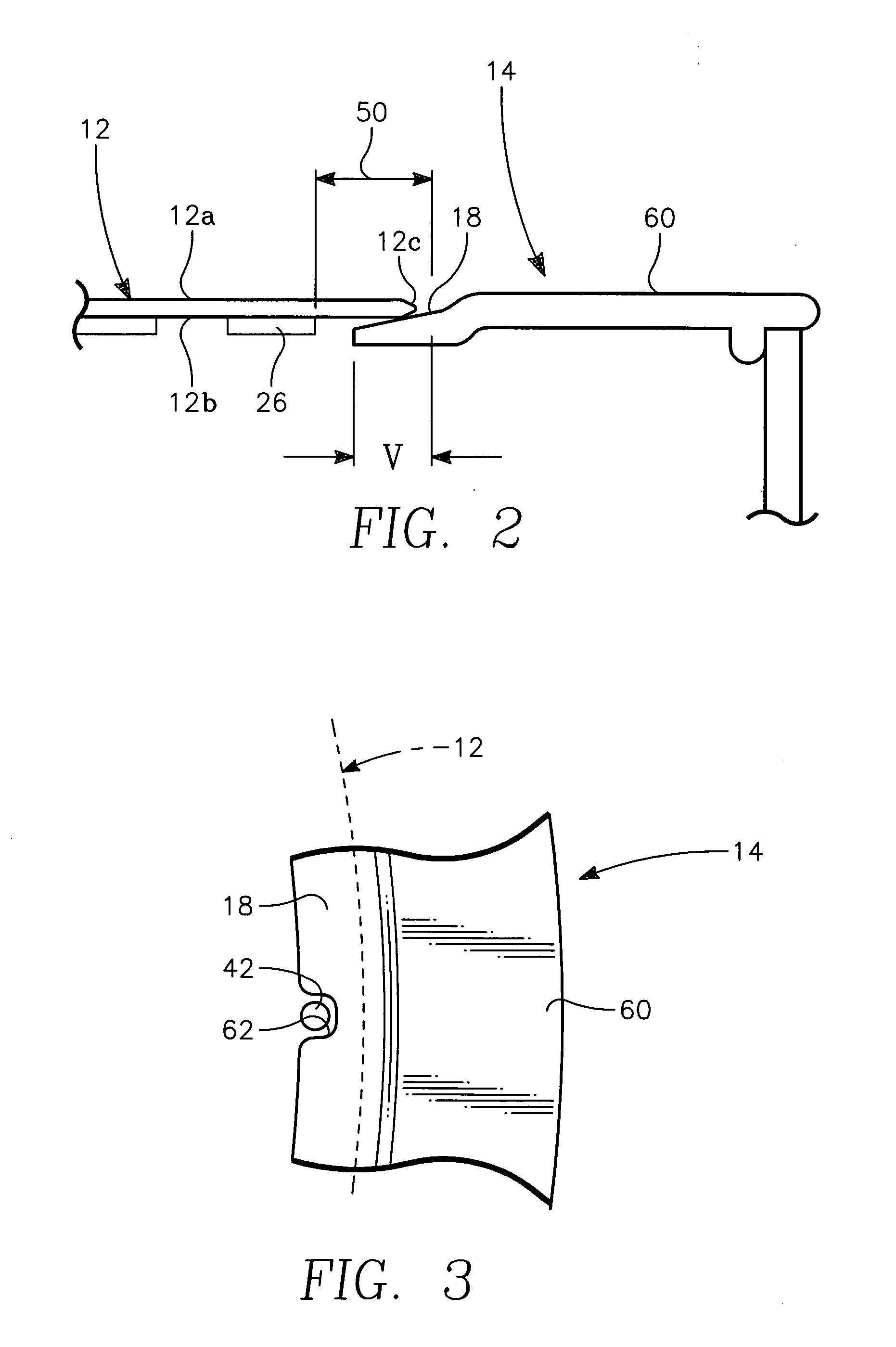
[0035]FIG. 5 shows a plan view of a wafer transfer apparatus 100 incorporating features of the present invention. Although the present invention will be described with reference to the embodiments shown in the drawings, it should be understood that this invention may be embodied in many alternate forms of embodiments. In addition, any suitable size, shape or type of elements or materials could be used. The wafer transfer apparatus 100 is adapted to transport wafers such as semiconductor wafers, such as silicon, gallium arsenide, semiconductor packaging wafers, such as high density interconnects, semiconductor manufacturing process imaging plates, such as masks or reticles, and large area, possibly rectangular, display panels, such as active matrix LCD panel, field emission arrays, plasma displays, other display panels or other applications such as solar cells.

[0036] As shown in FIG. 5, the wafer transfer apparatus 100 includes a wafer blade 102 configured to transfer the wafer 12 i...


PUM

PropertyMeasurementUnit
temperatureaaaaaaaaaa
diameteraaaaaaaaaa

Abstract

Three wafer support fixtures transfer a wafer for thermal processing in an inverted orientation within a heating chamber. Two co-planar support fixtures grab the wafer edge inside the chamber from a blade within a 1.5 mm wafer exclusion zone and hold it above the edge ring during heat-up and then withdraw thermal processing. A third support fixture chucks the wafer backside and transfers it to sloping support areas of the edge ring. The three support fixtures inside the chamber are individually controlled from outside. Alternatively, an arm connected to a controller is connected to the three support fixtures

Description

FIELD OF THE INVENTION [0001] This invention relates generally to heat treatment of semiconductor wafers and other substrates. In particular, the invention relates to a method and apparatus for transferring a wafer within a heating chamber in a rapid thermal processing system as well as other wafer processing systems. BACKGROUND ART [0002] The fabrication of integrated circuits from silicon or other wafers or different types of substrates such as glass flat panel displays or solar cells involves many steps of depositing layers and photo lithographically patterning the layers. Ion implantation may be used to dope active regions in the semiconductive silicon. The fabrication sequence also includes thermal annealing of the wafers or other substrates for many uses including curing implant damage and activating the dopants, crystallization, thermal oxidation and nitridation, silicidation, chemical vapor deposition, vapor phase doping, thermal cleaning, and other processesreasons. Althoug...

Claims


Application Information

Patent Timeline
Patent Type & Authority Applications(United States)
IPC IPC(8): B32B3/02C23C16/00
CPCH01L21/67115Y10T428/21H01L21/68707
Inventor ADERHOLD, WOLFGANGTROWBRIDGE, TERESA
Owner APPLIED MATERIALS INC
Features
  • Generate Ideas
  • Intellectual Property
  • Life Sciences
  • Materials
  • Tech Scout
  • Unparalleled Data Quality
  • Higher Quality Content
  • 60% Fewer Hallucinations
Learn More