Display Device

a display device and driver technology, applied in the field of display devices, can solve the problems of increasing the load per one ic chip and the liable increase of the generation of heat by the driver ic, and achieve the effects of high reliability, efficient heat radiating from the driver ic without restricting a degree of device design freedom, and efficient realization of impact resistan

Inactive Publication Date: 2007-09-20
HITACHI DISPLAYS
View PDF2 Cites 24 Cited by
  • Summary
  • Abstract
  • Description
  • Claims
  • Application Information

AI Technical Summary

Benefits of technology

[0019] Along with the realization of finer display cells and the higher packaging density of a driver IC for driving a recent flat panel display device, a demand for outputting signals to a larger number of electrodes with one IC chip is increasing. As a result, a load per one IC chip is increased and hence, the driver IC is liable to increase the generation of heat. Accordingly, to protect the driver IC from the thermal breakdown by rapidly suppressing the generation of heat of the driver IC thus maintaining the driver IC at a fixed temperature or below, there has been a demand for the development of the peripheral structure of the driver IC which can enhance the heat radiation efficiency using a simple technique.
[0020] Conventionally, as one means which can efficiently radiate heat of the driver IC without increasing the number of parts, as described in JP-A-10-260641, there has been proposed a method in which a portion of an aluminum reinforcing plate which supports a display panel from a back surface extends from an outer peripheral portion of the display panel, an IC chip is fixed to the portion, and the display panel is adhered to the aluminum reinforcing plate by way of a heat conductive adhesive transfer tape. Further, as described in JP-A-2000-268735, there has been proposed the constitution in which out of a pair of glass substrates which are adhered to each other, one glass substrate extends to the outside of another glass substrate, a heat radiation conductive pattern portion is formed on the extended portion and a driver IC is brought into contact with the conductive pattern and hence, heat generated by the IC chip is directly transferred to the glass substrate and the aluminum reinforcing plate thus enhancing the heat radiation property.

Problems solved by technology

As a result, a load per one IC chip is increased and hence, the driver IC is liable to increase the generation of heat.

Method used


Image

  • Display Device
  • Display Device
  • Display Device

Examples


embodiment 1

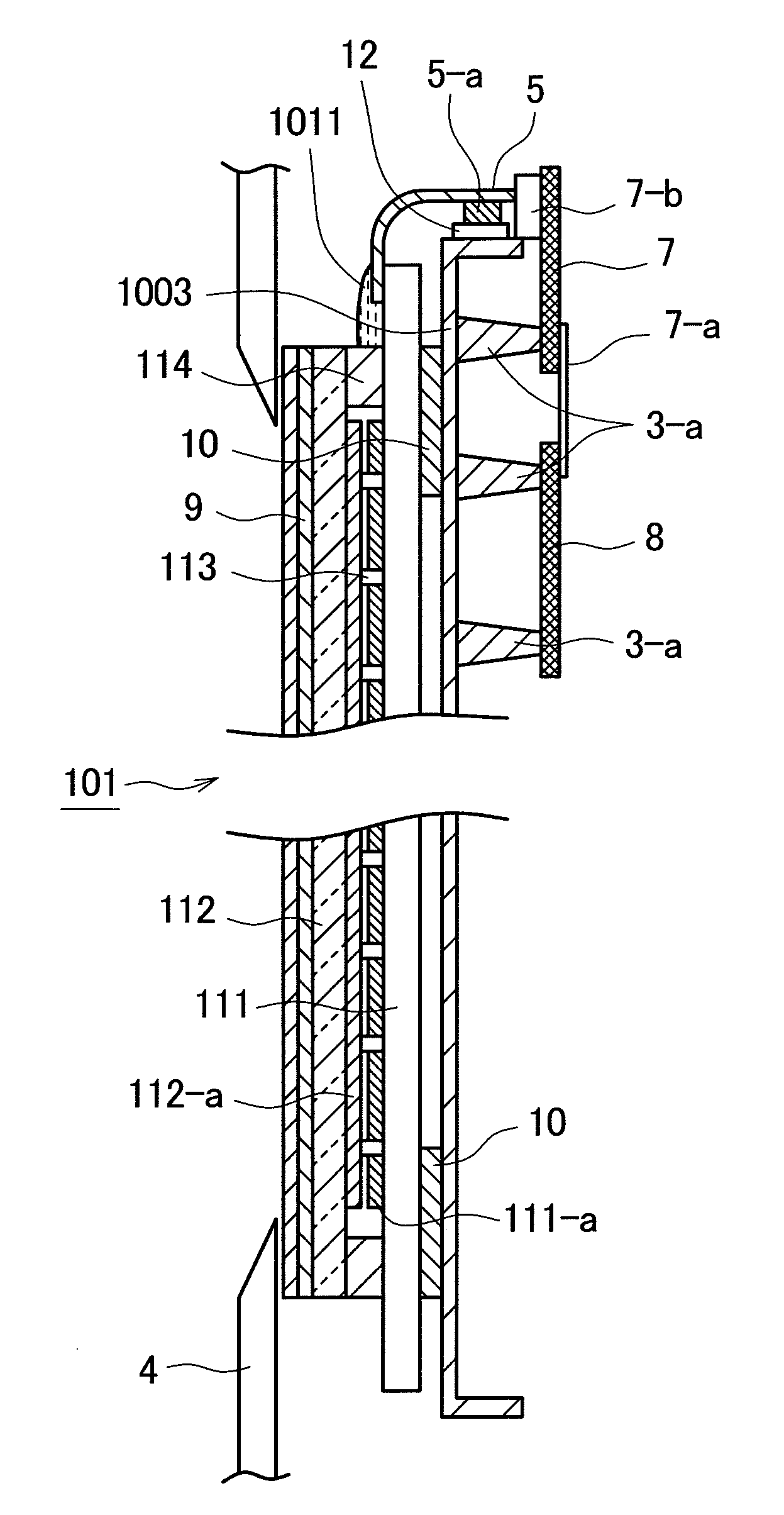
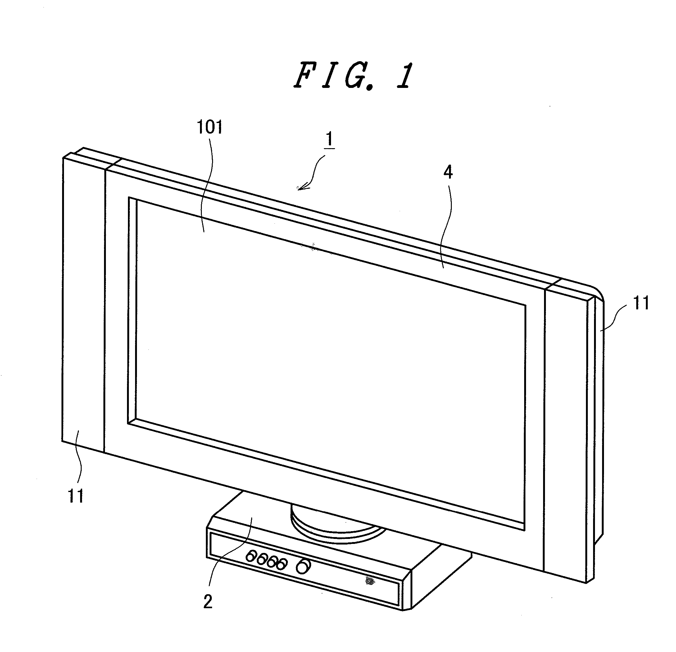
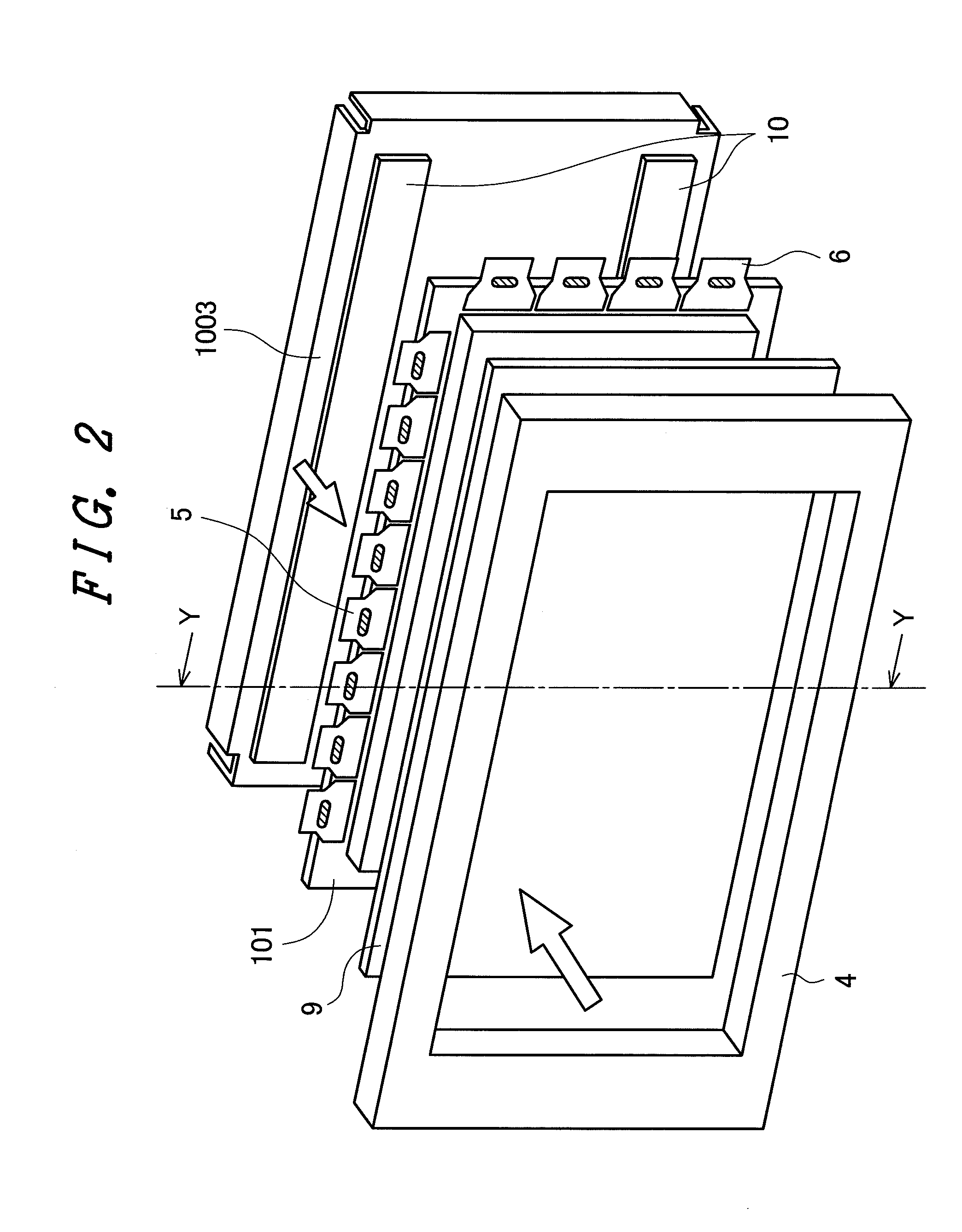
[0070] An embodiment 1 according to the present invention is explained in conjunction with FIG. 1 to FIG. 7. The present invention is explained in order from FIG. 1. FIG. 1 is a perspective view showing the schematic appearance of a display device of the embodiment 1 according to the present invention. In FIG. 1, the display device 1 is placed in a state that the display device 1 is supported on a display device support base 2. The display device 1 is used in a mode that an image such as a television image is displayed on a display panel 101 of the display device 1. The display panel 101 of the display device 1 uses a built-in electron emission display (FED). The display of an image on the display device 1 is performed in response to signals from a tuner unit or a video reproducing unit mounted in the inside of the display device support base 2. Further, speakers 11 are provided on the left and right sides of the display device 1 and hence, the display device 1 can also output sound...

embodiment 2

[0080] An embodiment 2 of the present invention is shown in FIG. 4. In place of adhering the driver IC 5-a to the outer wall formed by folding the peripheral end portion of the reinforcing member 1003, this embodiment 2 adopts a technique in which the driver IC 5-a is sandwiched between the reinforcing member 1003 and another metal plate 13 from the outside the outer wall of the reinforcing member 1003 and the driver IC 5-a is fixed using screws 14. A silicone sheet12 which possesses high thermal conductivity is interposed between the reinforcing member 1003 and the driver IC 5-a on a side with which the front surface of the driver IC 5-a is brought into contact and hence, the adhesiveness is enhanced thus providing the structure which can realize the more uniform heat radiation. Further, input terminals of the FPCs 5 for driving data electrode on a side opposite to the panel may be connected to the IF substrate 7 by thermo compression bonding in the same manner as the connection of...

embodiment 3

[0083]FIG. 5 shows an embodiment 3 which is a developed mode of the embodiment 2. In the embodiment 3, fins for enlarging a heat radiation are a are integrally formed on the metal plate 13 which fixes the driver IC 5-a by sandwiching the driver IC 5-a between the metal plate 13 and the reinforcing member 1003. Due to such constitution, it is possible to enhance the heat radiation efficiency compared to the embodiments 1, 2. Further, it may be possible to generate a convection which flows upwardly along the back surface side of the reinforcing member 1003 by forming spaces having some volume on back surfaces of the display panel 101 and the reinforcing member 1003 and by arranging a printed circuit board while taking the temperature elevation of the printed circuit board into consideration. In this case, it is possible to achieve the heat radiation more effectively by bringing the convection of air into direct contact with the metal plate 13 which forms the fins thereon. Accordingly,...


PUM


Abstract

The present invention ensures the efficient radiation of heat of a flat display panel without increasing a space outside a display screen of the flat display panel. A periphery of a reinforcing member adhered to a back surface of the flat display panel is folded in an L-shape and a driver IC is brought into contact with the folded portion.

Description

CLAIM OF PRIORITY [0001] The present application claims priority from Japanese Application JP 2006-070545 filed on Mar. 15, 2006, the content of which is hereby incorporated by reference into this application. BACKGROUND OF THE INVENTION [0002] 1. Field of the Invention [0003] The present invention relates to a display device which displays a television image or the like using a planar display panel (flat panel: FPD). [0004] 2. Description of Related Arts [0005] Recently, with respect to a display device such as a television receiver set, along with the progress of a display device such as a liquid crystal panel (herein after abbreviated as LCD), a plasma display panel (herein after abbreviated as PDP) and an electric-field or electron-emission display (Field Emission Display: herein after referred to as FED), techniques for making the display flat and thin have been rapidly developed. [0006] Such a flat-panel display device such as the LCD, the PDP or the FED adopts the following s...

Claims


Application Information

Patent Timeline
Patent Type & Authority Applications(United States)
IPC IPC(8): G09G5/00
CPCG09G3/006G09G2320/041G09G2300/04G09G3/22G02F1/13452H05K7/20963
Inventor YATSU, YASUHARUOSAWA, ATSUOSHIRAISHI, MIKIOKODERA, YOSHIEOHISHI, TETSU
Owner HITACHI DISPLAYS
Why Eureka
Try Eureka