Method and device for detecting DNA using surface-treated nanopore

a nanopore and surface-treated technology, applied in the field of methods and devices for detecting nucleic acids using nanopores, can solve the problems of difficult detection of dna less than 2000 base pairs (bps), high difficulty, and high passage rate of dna through the nanopor

Inactive Publication Date: 2007-09-20
SAMSUNG ELECTRONICS CO LTD
View PDF19 Cites 58 Cited by
  • Summary
  • Abstract
  • Description
  • Claims
  • Application Information

AI Technical Summary

Benefits of technology

[0012] In an exemplary embodiment, the surface of a nanopore is treated with a substance carrying positive (+) charges to change the surface property of the nanopore. Treatment of substance carrying positive (+) charges to the nanopore surface renders the surface to carry positive (+) charges. Such treatment increases the interaction between the nanopore and DNA passing through said nanopore, thus allowing detection of DNA even with a nanopore having a relatively large diameter.

Problems solved by technology

However, such prior-art DNA detection methods and systems that use nanopores raise problems, because when these methods are applied, the detection of DNA having a size less than 2000 base pairs (bps) becomes difficult.
Such difficulty rises from the extremely high passage rate of DNA through the nanopore.
Other problems include the complicated structure of the DNA detection system and the difficulty of maintaining an appropriate DNA detection condition, mainly maintaining the diameter of the nanopore at less than 10 nm and preferably less than 5 nm.
Although many efforts have been made to form nanopores with a diameter as small as that of bio-pores, various problems resulting from the difficulty of forming such nanopores have been raised.

Method used


Image

  • Method and device for detecting DNA using surface-treated nanopore
  • Method and device for detecting DNA using surface-treated nanopore
  • Method and device for detecting DNA using surface-treated nanopore

Examples


example 1

[0047] 1. Formation of Solid Substrate having 30 nm Diameter Nanopore

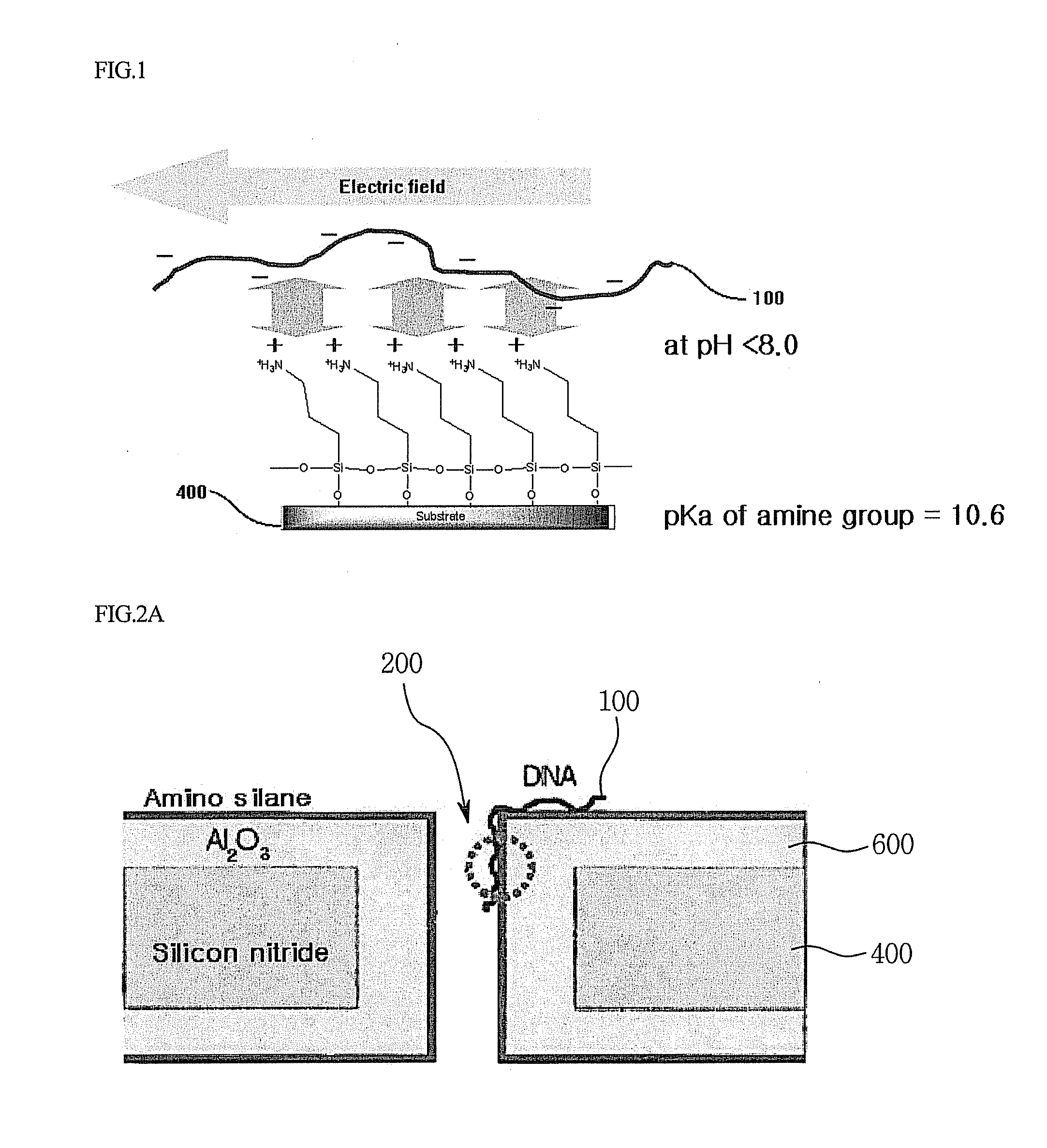
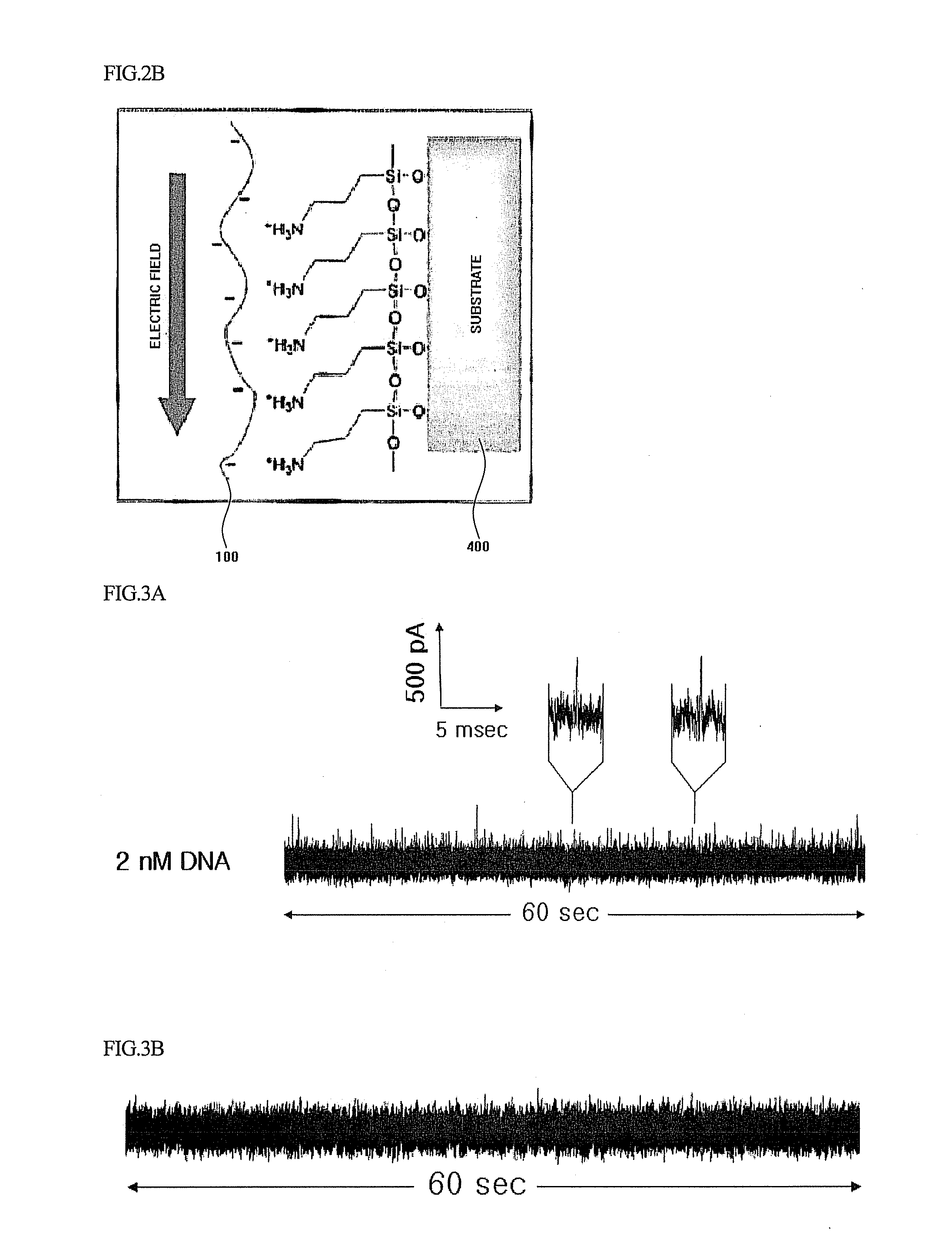
[0048] A 250 nm silicon nitride was deposited on silicon substrate using low pressure chemical-vapor deposition (“LPCVD”). A thin free standing membrane of silicon nitride having a size of 30μm× 30 μm (Length×Width) was fabricated by opening a window in the unpolished side of the substrate using photo lithography, followed by reactive ion etching and KOH wet etching to remove the silicon. Then, a 100 nm diameter pore was formed in the central portion of the membrane using a FIB machine (focused ion beam machine) SMI2050 (manufactured by Seiko instrument Inc.). and a thin layer made of aluminum oxide (Al203) was deposited into the pore using atomic layer deposition so that the diameter of the pore was reduced to a size of 30 nm. The thickness of the deposited A12O3 layer was measured with an ellipsometer. As a result, a cylindrical nanopore having a diameter of 30 nm was formed through the 320 nm thick membrane.

[0...

example 2

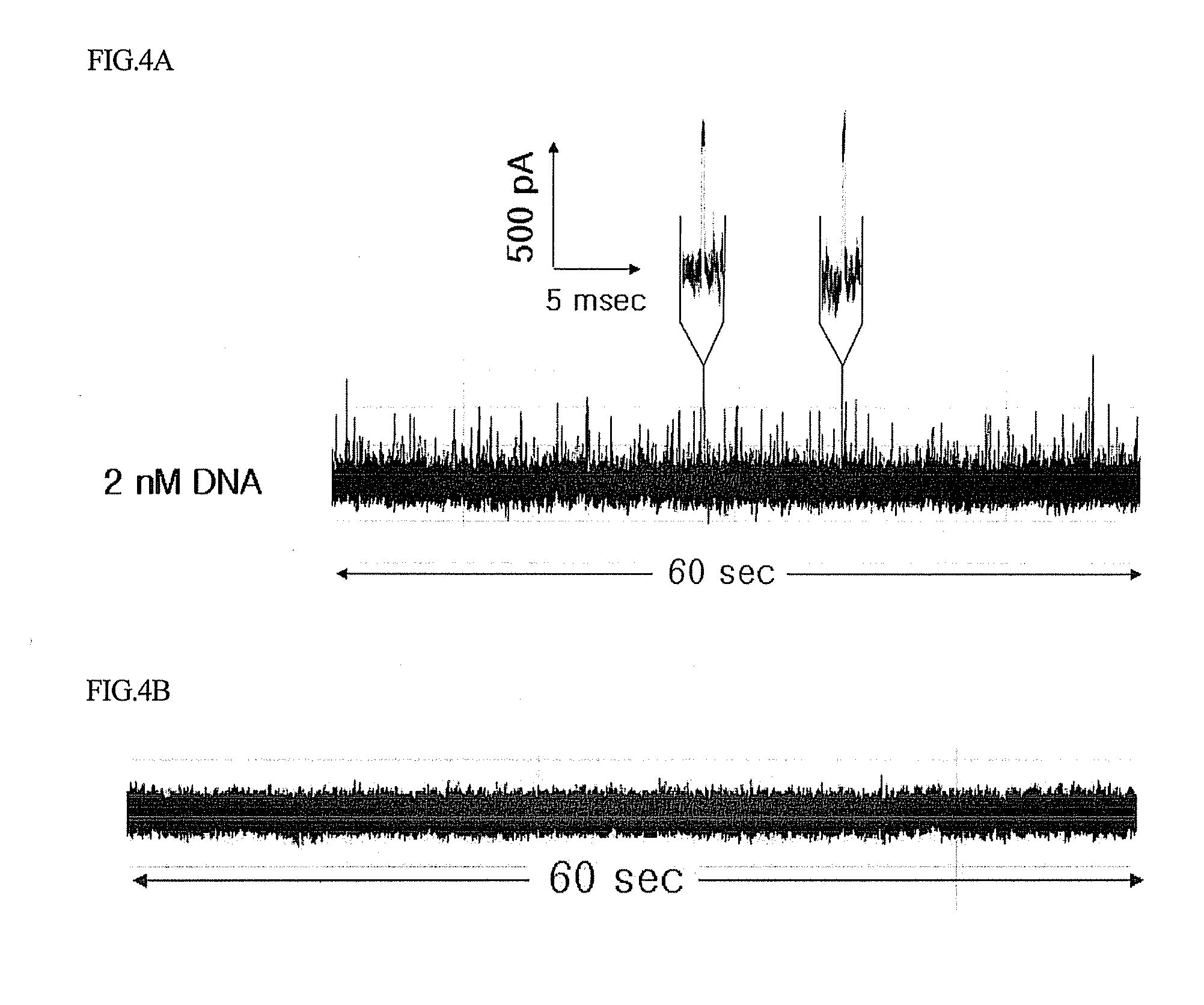
Example 2 was performed in the same manner as in Example 1, except that the double-stranded DNA loaded into the inventive device had a size of 910 bps. The measurement results are shown in FIG. 4A.


PUM

PropertyMeasurementUnit
sizeaaaaaaaaaa
diameteraaaaaaaaaa
diameteraaaaaaaaaa

Abstract

Disclosed herein is a method for detecting DNA using a nanopore including treating the surface of a nanopore formed in a solid substrate with a substance carrying positive charges; introducing a DNA-containing sample into the surface-treated nanopore; and detecting electrical signals generated during translocation of the sample through the nanopore. Also disclosed herein is device for detecting DNA using a nanopore including a solid substrate including a nanopore, treated with a substance which carries positive charges to change a surface property of the nanopore so that the nanopore surface carries positive charges; an electrode applying voltage to the nanopore of the solid substrate; and a measurement unit measuring an electrical signal generated during translocation of a DNA-containing sample through the nanopore.

Description

[0001] This application claims priority to Korean Patent Application No. 10-2005-0097648, filed Oct. 17, 2005, and all the benefits accruing therefrom under 35 U.S.C. § 119, the contents of which in its entirety are herein incorporated by reference. BACKGROUND OF THE INVENTION [0002] 1. Field of the Invention [0003] The present invention relates to a method and device for detecting nucleic acids using a nanopore. More particularly, the invention relates to a method and device for detecting DNA without special labeling by using a nanopore, which may detect DNA having a size of less than 1 kilo-base-pairs (“kbps”) using a nanopore having changed surface properties, without special labeling. [0004] 2. Description of the Prior Art [0005] Various methods for detecting target biomolecules in samples have been developed. Among these methods, the method of using nanopores for detection is now being considered as a high-sensitivity DNA detection system that may be similar to the method of us...

Claims


Application Information

Patent Timeline
Patent Type & Authority Applications(United States)
IPC IPC(8): C12Q1/68C12M3/00
CPCC12Q1/6825G01N33/48721C12Q2565/631
Inventor KIM, YOUNG ROKMIN, JUN HONGLEE, IN HOKIM, AH GIKIM, KUI HYUN
Owner SAMSUNG ELECTRONICS CO LTD
Why Eureka
Try Eureka