Touch Sensitive Display

a display and touch technology, applied in the field of touch sensitive display, can solve the problems of significant increase in the thickness of the resulting touch sensitive display, high accuracy, and significant progress in the user interface, so as to reduce the thickness, reduce manufacturing costs, and improve the effect of accuracy

Inactive Publication Date: 2007-09-27
KONINKLIJKE PHILIPS ELECTRONICS NV
View PDF1 Cites 106 Cited by
  • Summary
  • Abstract
  • Description
  • Claims
  • Application Information

AI Technical Summary

Benefits of technology

[0027] A particular advantage of the present invention is that a touch sensitive display having reduced thickness is achieved. A further advantage is reduced manufacturing costs for touch sensing displays, since both driving circuitry and touch sensing circuitry can be made on the active substrate in the same process. A further advantage is high accuracy and high resolution of detection of a touched point, since each touch sensing circuitry can be associated with a pixel. A further advantage is maintained resolution and definition of the displayed image when introducing touch sensing features in an active matrix (AM) display technology. These multi-layer thin-film AM technologies are attractive because of the possibility to integrate the display drivers, the peripheral driving electronics, and additional functionalities, for example a touch sensitive element, into the display itself.
[0028] According to another feature of the invention, the detection means is operable to detect a plurality of simultaneous touch points. Preferably the detection means can simultaneously detect changed capacitances between a plurality of pairs of first and second electrodes. This is possible due to the active matrix structure of the display and its integrated touch sensors. An advantage of this is increased flexibility and improved functionality of a device comprising the touch sensitive display.
[0029] According to a different feature of the invention, a plurality of touch sensors is aligned with a corresponding plurality of pixels of the active matrix display. This may allow for a very simple and accurate correspondence between touch sensitive elements and a displayed image and may obviate or mitigate the requirement for calibration. Preferably, the alignment is achieved by aligning the touch sensitive elements with the storage capacitor and / or sacrificial TFT of the active matrix display element.
[0030] According to a feature of the invention, the touch sensitive element comprises a Micro-Electromechanical (MEM) capacitor or sacrificial TFT operable to modify their capacitance. This allows for a particularly suitable implementation. Specifically, it provides process compatibility. Thus, reduced manufacturing complexity and cost for touch sensitive displays, e.g. amorphous silicon based active matrix displays, are achieved.

Problems solved by technology

In addition, the user interface has progressed significantly and much effort has been put into providing an intuitive interaction mechanism.
The display device comprises a number of layers resulting in a significant increase in the thickness of the resulting touch sensitive display.
This degrades the optical performance of the touch sensitive display and requires that materials having suitable optical properties are used to implement the touch screen.
A problem is that the performance of the touch sensitive display of the prior art do not meet requirements of spatial resolution, low thickness, and visual performance.

Method used


Image

  • Touch Sensitive Display
  • Touch Sensitive Display
  • Touch Sensitive Display

Examples


Embodiment Construction

[0039] The drive for displays capable of combining high performance, high-speed video, large size and low power, pushes display technology into the direction of Active Matrix (AM) Liquid Crystal Display (LCD) technologies. The present invention is applicable to various active matrix display devices. The following specific embodiments will describe the invention in relation to an active matrix liquid crystal display (AMLCD) device by way of example only. It will be appreciated that other types of active matrix display devices can be employed, e.g. devices using electrophoretic ink, polyLED, OLED, plasma display, and flexible version thereof.

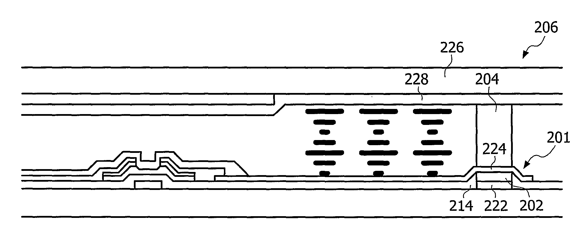
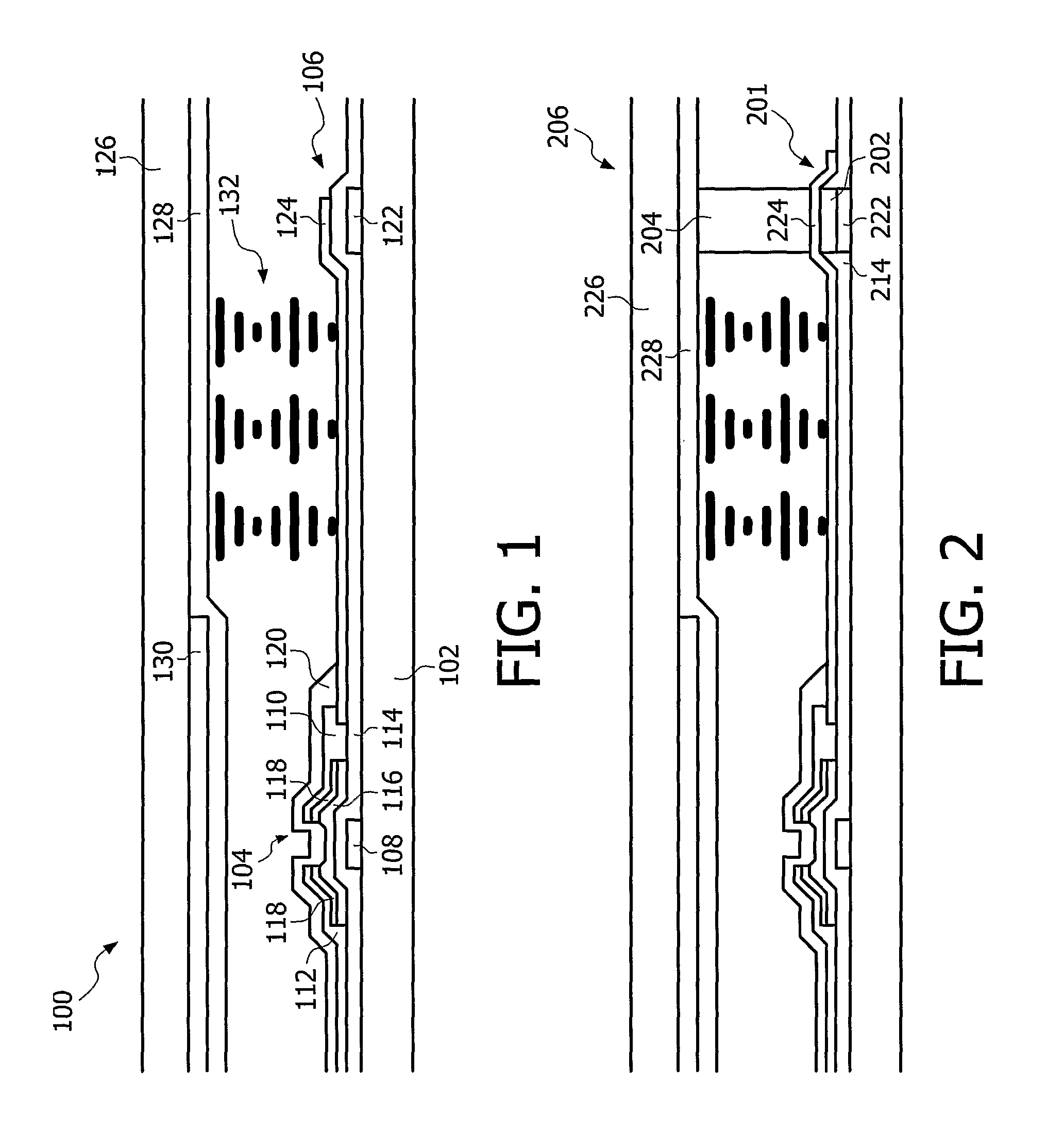
[0040] In order to illustrate the integration of touch-sensing features into an AMLCD technology, reference is made to FIG. 1 showing a schematic cross sectional view of a typical AMLCD 100. A liquid crystal 132 is sandwiched between a passive substrate 126 and an active substrate 102. Furthermore, each pixel is provided with a driving TFT 104 an...


PUM

PropertyMeasurementUnit
dielectric constantaaaaaaaaaa

Abstract

There is provided a touch sensitive display comprising a passive substrate, an active substrate, and a display material disposed between the passive and active substrates, wherein driving circuitry for driving a pixel of the display and touch sensing circuitry are arranged on the active substrate. The touch sensing circuitry comprises at least one component with a first and a second electrode, wherein the electrodes are arranged to displace with respect to each other in response to a touch input.

Description

FIELD OF INVENTION [0001] The present invention relates to a touch sensitive display. BACKGROUND OF INVENTION [0002] The market for handheld and portable consumer electronics and computing has significantly diversified in the last decade. The trend has increasingly been towards smaller devices capable of displaying increasing amounts of information leading to improved displays having higher resolutions. [0003] In addition, the user interface has progressed significantly and much effort has been put into providing an intuitive interaction mechanism. A frequently used method for receiving user inputs is by incorporating a touch screen at the device. This allows for a user interaction by the user touching a touch sensitive display. [0004] WO 03 / 079449 A1 discloses an AM electroluminescent display device comprising a pressure sensor structure comprising a transparent upper electrode layer, an underlying conductive barrier layer, and a compressible layer of dielectric or highly resistive...

Claims


Application Information

Patent Timeline
Patent Type & Authority Applications(United States)
IPC IPC(8): G06F3/033G02F1/133G06F3/041G06F3/044
CPCG06F3/0412G02F1/13394G06F3/044G06F3/0445G02F1/133
Inventor VAN DELDEN, MARTINUS HERMANUS WILHELMUS MARIAVAN BEEK, JOZEF THOMAS MARTINUSDESTURA, GALILEO JUNE ADEVAKEMMEREN, ANTONIUS LUCIEN ADRIANUS MARIA
Owner KONINKLIJKE PHILIPS ELECTRONICS NV
Why Eureka
Try Eureka