Semiconductor device using semiconductor nanowire and display apparatus and image pick-up apparatus using the same

a semiconductor nanowire and semiconductor technology, applied in the field of semiconductor nanowire devices, can solve problems such as complex apparatus structure, and achieve the effect of complex apparatus structur

Inactive Publication Date: 2007-10-04
CANON KK
View PDF3 Cites 64 Cited by
  • Summary
  • Abstract
  • Description
  • Claims
  • Application Information

AI Technical Summary

Benefits of technology

[0021] According to the present invention, a function materialized by a semiconductor junction such as a PN junction or a PIN junction and an FET function can be exhibited at the same time. Further, it is possible to make small a connection resistance between a junction region such as a PN junction and a PIN junction and an FET region. Therefore, when a light-emitting device or a light-receiving device is formed with a semiconductor junction region such as a PN junction region, the light-emitting efficiency and a photoelectric conversion efficiency of the device as a whole can be made high.

Problems solved by technology

However, in a conventional technique, when a display apparatus or an image pick-up apparatus is required to be formed using nanowires, switching portions (for example, field effect transistors) have to be provided separately, causing a problem in that a structure of the apparatus becomes complicated.

Method used


Image

  • Semiconductor device using semiconductor nanowire and display apparatus and image pick-up apparatus using the same
  • Semiconductor device using semiconductor nanowire and display apparatus and image pick-up apparatus using the same
  • Semiconductor device using semiconductor nanowire and display apparatus and image pick-up apparatus using the same

Examples


embodiments

[0068] Although the following is a specific description of embodiments according to the present invention, the present invention is not limited thereto.

first embodiment

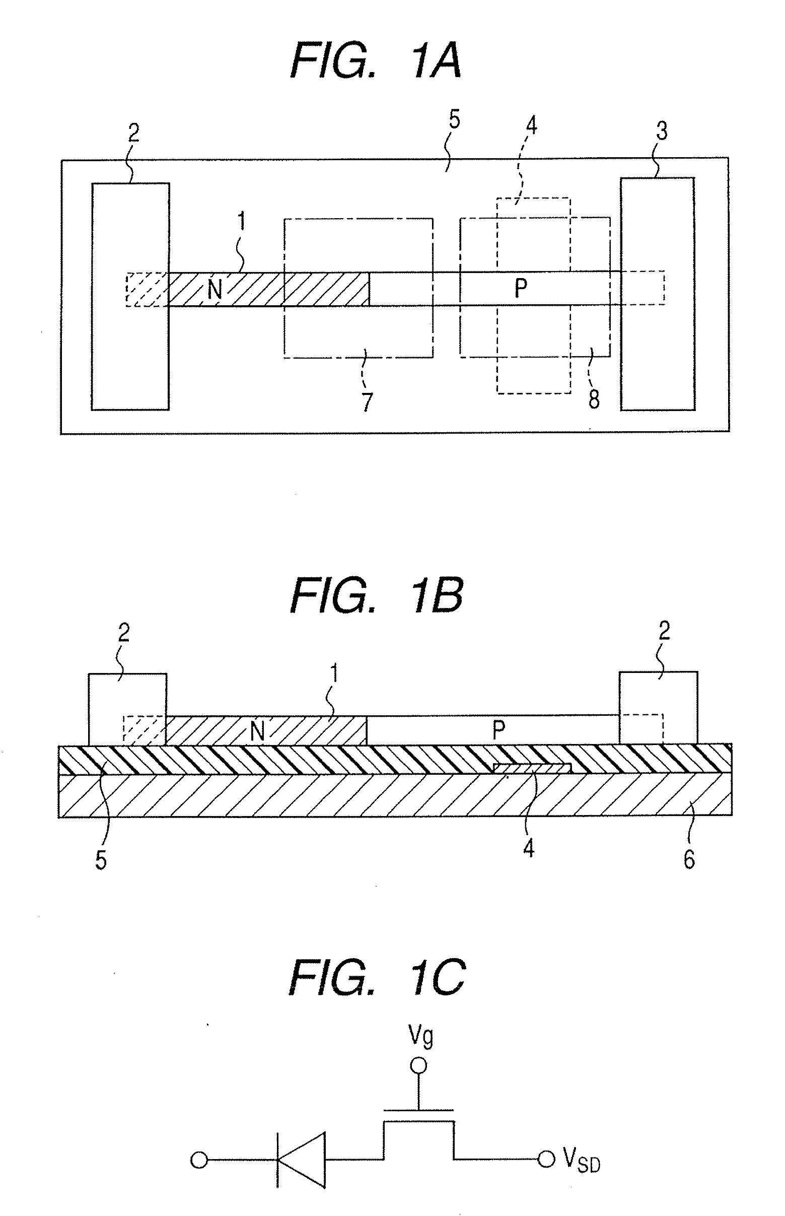
[0069] In this embodiment, a case where the present invention is applied to a display apparatus is shown. Here, semiconductor nanowires made of GaN are used. The nanowires are manufactured by the VLS mechanism.

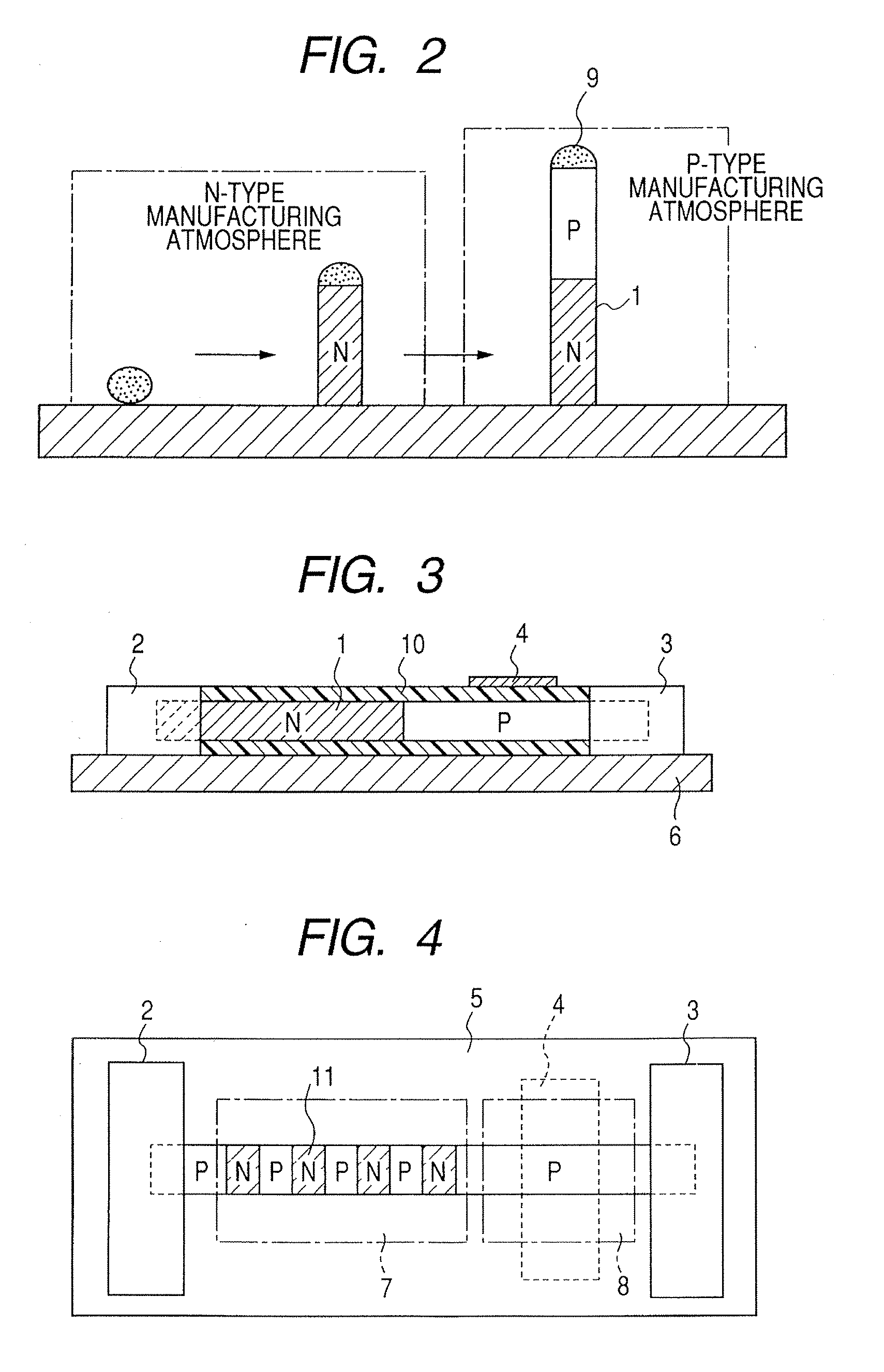
[0070] The method of manufacturing the display apparatus is as follows. First, Au fine particles having a particle size of 50 nm are formed on a sapphire substrate. After that, the substrate is heated to 900° C. in an atmosphere of trimethylgallium (TMGa) and ammonia to manufacture GaN nanowires to be a buffer layer.

[0071] Then, in order to manufacture N-type GaN thereon, the nanowires are grown in an atmosphere of trimethylgallium (TMGa), silane gas, and ammonia to manufacture an n-GaN:Si layer. Then, as an active layer, an InGaN layer is manufactured thereon in an atmosphere of trimethylgallium (TMGa), trimethylindium (TMIn), and ammonia. Then, in order to manufacture P-type GaN, the substrate is heated to 900° C. in an atmosphere of cyclopentadienylmagnesium (Cp2Mg) gas, ...

second embodiment

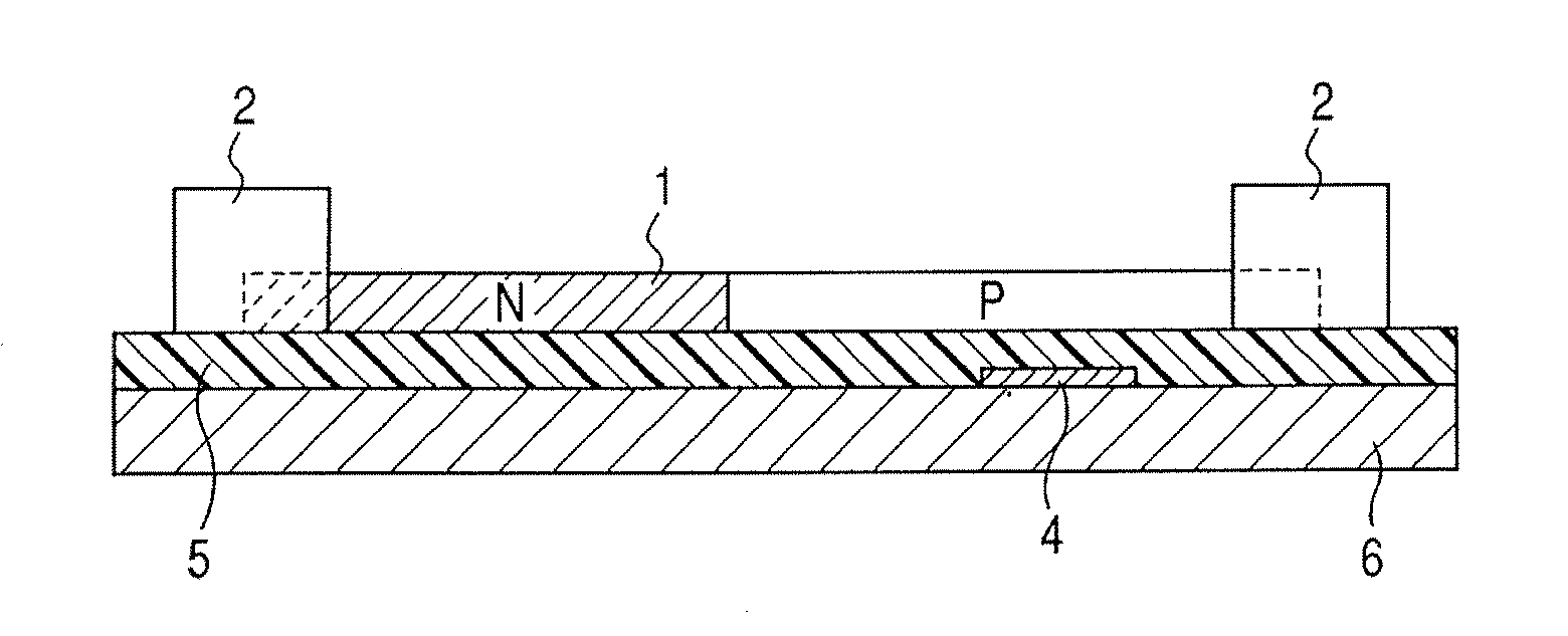
[0075] In this embodiment, a case where the present invention is applied to a two-dimensional display sensor is shown. Here, semiconductor nanowires made of silicon are used. The nanowires are manufactured by the VLS mechanism. The method of manufacturing the two-dimensional display sensor is as follows. First, Au fine particles having a particle size of 50 nm are formed on a silicon substrate. After that, the substrate is heated to 450° C. in an atmosphere of SiH4 and PH3 gas to form P-doped N-type Si nanowires. Then, the substrate is heated at 450° C. in an atmosphere of SiH4 and B2H6 gas to form P-type Si nanowires on the N-type Si nanowires. Finally, by carrying out annealing at 500° C. in an atmosphere of nitrogen, photodiode nanowires having PN junctions are obtained. The respective thickness of the nanowires obtained as described above are about 10 μm for the N-type and about 30 μm for the P-type. The nanowires obtained by the above-mentioned method are dispersed in an ethano...


PUM


Abstract

A semiconductor device, comprising a semiconductor nanowire having a first region with one of a PN junction and a PIN junction and a second region with a field effect transistor structure, a pair of electrodes connected to both ends of the semiconductor nanowire, and a gate electrode provided in at least a part of the second region via an insulating layer. The semiconductor nanowire has a P-type semiconductor portion and an N-type semiconductor portion, and one of the P-type semiconductor portion and the N-type semiconductor portion is a common structural element of both the first and second regions.

Description

BACKGROUND OF THE INVENTION [0001] 1. Field of the Invention [0002] The present invention relates to a semiconductor device using a semiconductor nanowire. [0003] Also, the present invention relates to a semiconductor device which has both a PN or PIN junction device and a field effect transistor using a semiconductor nanowire. Further, the present invention relates to a display apparatus and an image pick-up apparatus using the semiconductor device. [0004] 2. Description of the Related Art [0005] A semiconductor nanowire is a wire exhibiting semiconductor characteristics and having a structure of a diameter of about several hundred nanometers or less. Such a semiconductor nanowire is manufactured using, for example, a vapor-liquid-solid (VLS) mechanism. [0006] The VLS mechanism is a method in which metal fine particles on a substrate and the substrate or a desired element form a molten compound alloy, which decomposes a raw material gas to allow a nanowire to grow. The VLS mechanis...

Claims


Application Information

Patent Timeline
Patent Type & Authority Applications(United States)
IPC IPC(8): H01L29/76
CPCB82Y10/00H01L27/14621H01L2924/0002H01L27/14643H01L27/14683H01L29/0665H01L29/0673H01L29/068H01L29/861H01L29/868H01L31/035281H01L33/18H01L33/20Y02E10/50H01L2924/00
Inventor SHIOYA, SHUNSUKEIKEDA, SOTOMITSU
Owner CANON KK
Why Eureka
Try Eureka