
Semiconductor device and a method of manufacturing the same

Active Publication Date: 2007-10-04
RENESAS ELECTRONICS CORP
View PDF1 Cites 55 Cited by
  • Summary
  • Abstract
  • Description
  • Claims
  • Application Information

AI Technical Summary

Benefits of technology

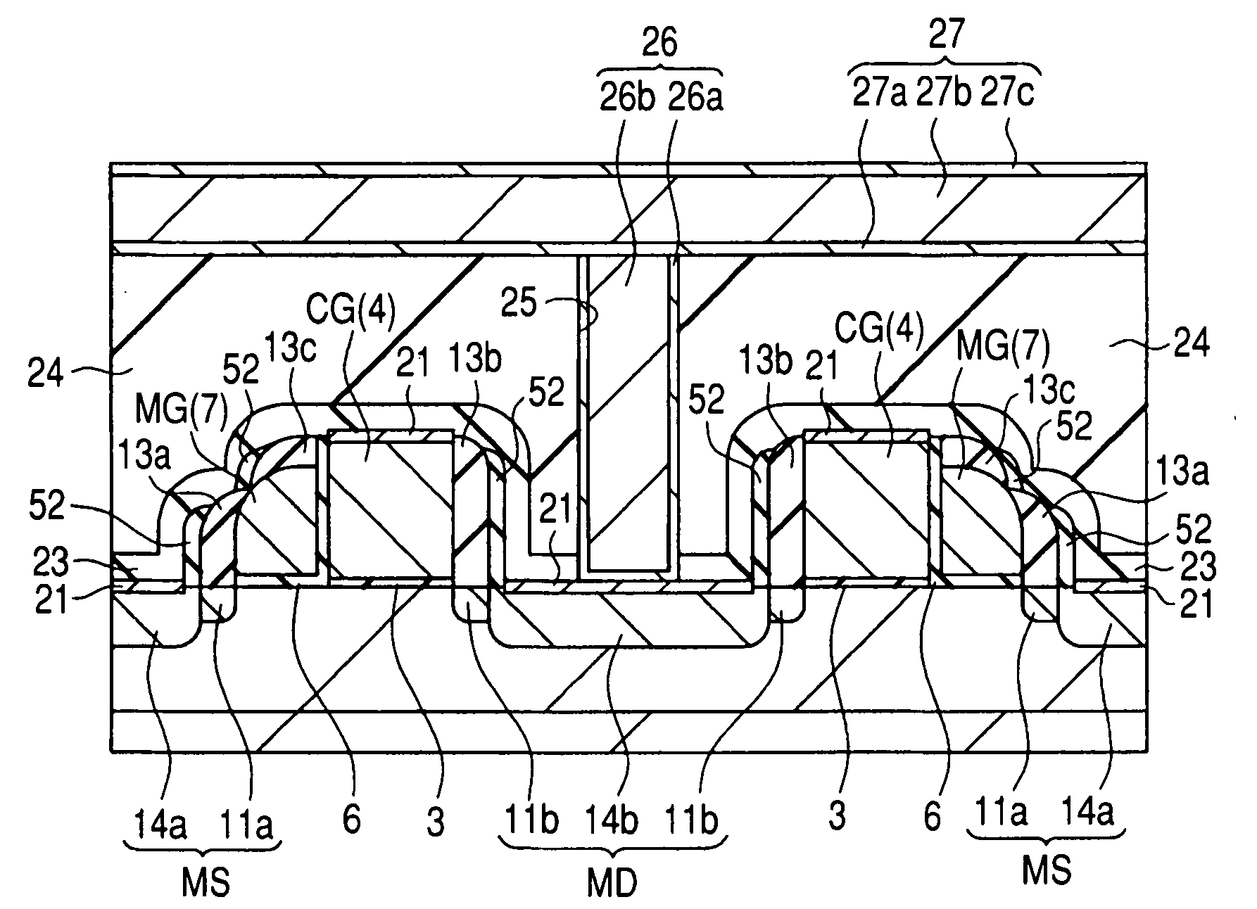
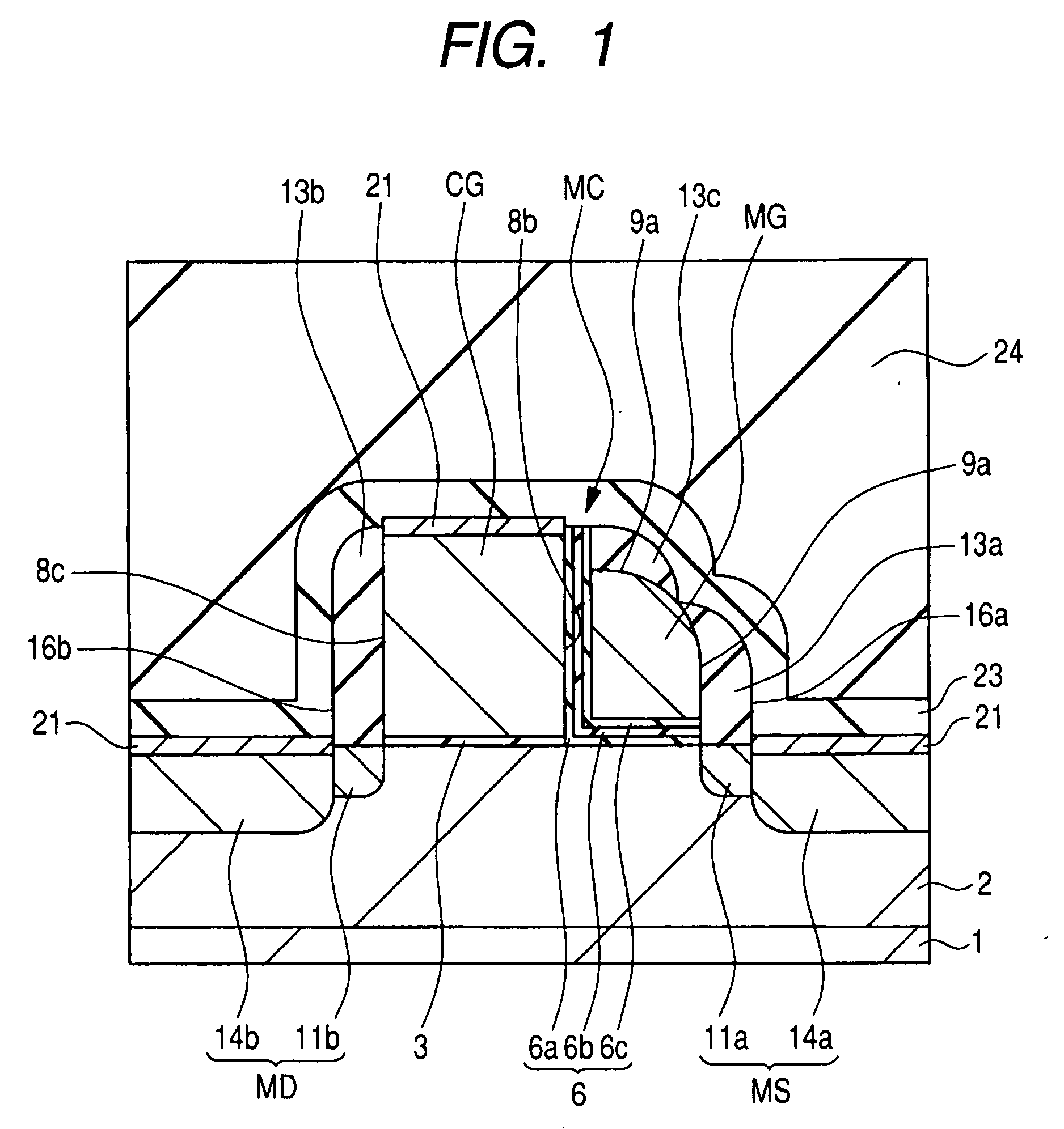
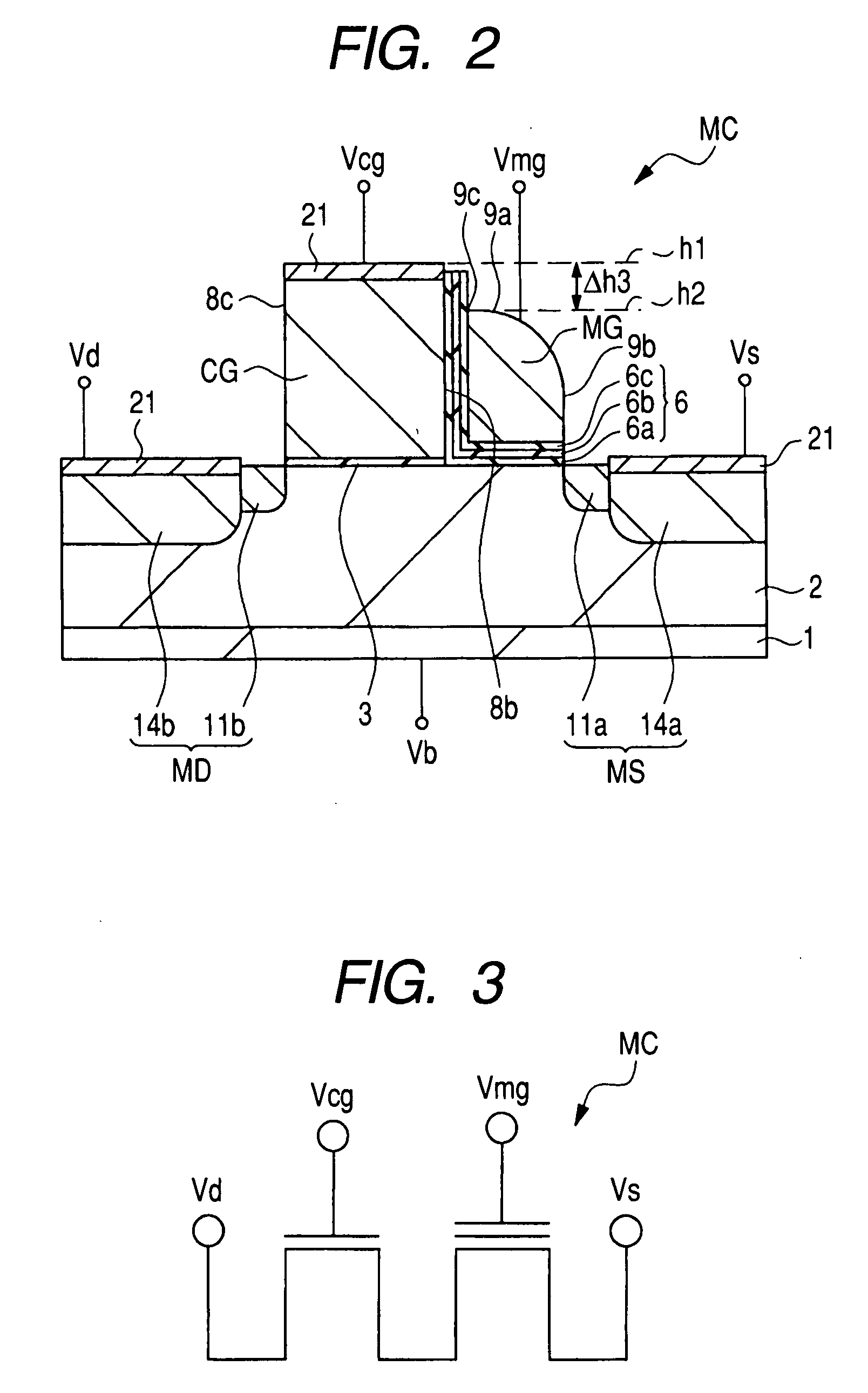
[0007]Formation of a metal silicide film such as cobalt silicide over the upper surfaces of the control gate electrode and memory gate electrode can be given as one measure for reducing the resistance between the control gate electrode and memory gate electrode, thereby increasing the speed of the memory operation. According to the investigation by the present inventors, however, when metal silicide films are formed over the upper surfaces of the control gate electrode and memory gate electrode, a short-circuit fault between the control gate electrode and memory gate electrode may presumably occur because owing to small thickness of the ONO film, the end portion of the metal silicide film over the control gate electrode domes close to the end portion of the metal silicide film over the memory gate electrode. The short circuit between the control gate electrode and memory gate electrode occurs, depending on the formation state of the respective metal silicide films over the control gate electrode and memory gate electrode. It occurs when the metal silicide film over the control gate electrode comes close, in the bridge form, to the metal silicide film over the memory gate electrode. A semiconductor device having such a short circuit fault must be selected and eliminated in the test during the fabrication of the semiconductor device. This deteriorates the production yield of the semiconductor device and heightens its cost (unit price).
[0009]An object of the present invention is to provide a technology capable of improving the production yield of a semiconductor device.

Problems solved by technology

According to the investigation by the present inventors, however, when metal silicide films are formed over the upper surfaces of the control gate electrode and memory gate electrode, a short-circuit fault between the control gate electrode and memory gate electrode may presumably occur because owing to small thickness of the ONO film, the end portion of the metal silicide film over the control gate electrode domes close to the end portion of the metal silicide film over the memory gate electrode.
This deteriorates the production yield of the semiconductor device and heightens its cost (unit price).
This may deteriorate the performance of a semiconductor device.

Method used


Image

  • Semiconductor device and a method of manufacturing the same
  • Semiconductor device and a method of manufacturing the same
  • Semiconductor device and a method of manufacturing the same

Examples


embodiment 1

[0050]The present invention mainly relates to a semiconductor device using a charge trap insulating film (an insulating film capable of accumulating charges therein) for a charge accumulator portion thereof so that in the below-described embodiment, a description will be made based on a memory cell having an n channel MISFET (MISFET: Metal Insulator Semiconductor Field Effect Transistor) as a basic structure and using a charge trap insulating film. In the below-described embodiment, the polarity (polarity of an applied voltage or polarity of the carrier during the program, erase and read operations) is for describing the operation of the memory cell having an n channel MISFET as a basic structure. When a memory cell has a p channel MISFET as a basic structure, similar operation is available in principle by reversing all the polarities of the applied voltage and conductivity type of the carrier.

[0051]A semiconductor device according to this Embodiment and a manufacturing method of th...


PUM


Abstract

Provided is a semiconductor device having, over a semiconductor substrate, a control gate electrode and a memory gate electrode which are adjacent to each other and constitute a nonvolatile memory. The height of the memory gate electrode is lower than the height of the control gate electrode. A metal silicide film is formed over the upper surface of the control gate electrode, but not formed over the upper surface of the memory gate electrode. The memory gate electrode has, over the upper surface thereof, a sidewall insulating film made of silicon oxide. This sidewall insulating film is formed in the same step as that for the formation of respective sidewall insulating films over the sidewalls of the memory gate electrode and the control gate electrode. The present invention makes it possible to improve the production yield and performance of the semiconductor device having a nonvolatile memory.

Description

CROSS-REFERENCE TO RELATED APPLICATIONS[0001]The disclosure of Japanese Patent Application No. 2006-103464 filed on Apr. 4, 2006 including the specification, drawings and abstract is incorporated herein by reference in its entirety.BACKGROUND OF THE INVENTION[0002]The present invention relates to a semiconductor device and a manufacturing method thereof, in particular, a technology effective when applied to a semiconductor device having a nonvolatile memory and a manufacturing method thereof.[0003]As an electrically programmable and erasable nonvolatile semiconductor memory device, EEPROM (Electrically Erasable and Programmable Read Only Memory) has been employed widely. Such a memory device (memory) typified by a flash memory which is used popularly now has, below a gate electrode of its MISFET, a conductive floating gate electrode encompassed by an oxide film or a charge trap insulating film. With the charge accumulation state in the floating gate or charge trap insulating film as...

Claims


Application Information

Patent Timeline
IPC IPC(8): H01L29/94H01L29/76H01L31/00
CPCH01L21/28282H01L27/115H01L29/7885H01L29/42324H01L29/42328H01L27/11521H01L29/40117H10B69/00H10B41/30
Inventor TOBA, KOICHIISHII, YASUSHIKAWASHIMA, YOSHIYUKIMACHIDA, SATORUNAKAGAWA, MUNEKATSUHASHIMOTO, TAKASHI
Owner RENESAS ELECTRONICS CORP
Learn More