
Charge pump circuit and method thereof

a charge pump and circuit technology, applied in the direction of electrical equipment, pulse automatic control, etc., can solve the problems of high circuit complexity, poor performance of the prior art charge pump circuit shown in fig. 1 and other problems, to achieve the effect of improving the efficiency of the pump, and improving the performance of the pll

Active Publication Date: 2007-10-04
REALTEK SEMICON CORP
View PDF9 Cites 8 Cited by
  • Summary
  • Abstract
  • Description
  • Claims
  • Application Information

AI Technical Summary

Benefits of technology

[0002] The prevent invention relates to charge pump circuit, more particularly, to method and apparatus for canceling mismatch and suppressing clock feedthrough for charge pump circuit.

Problems solved by technology

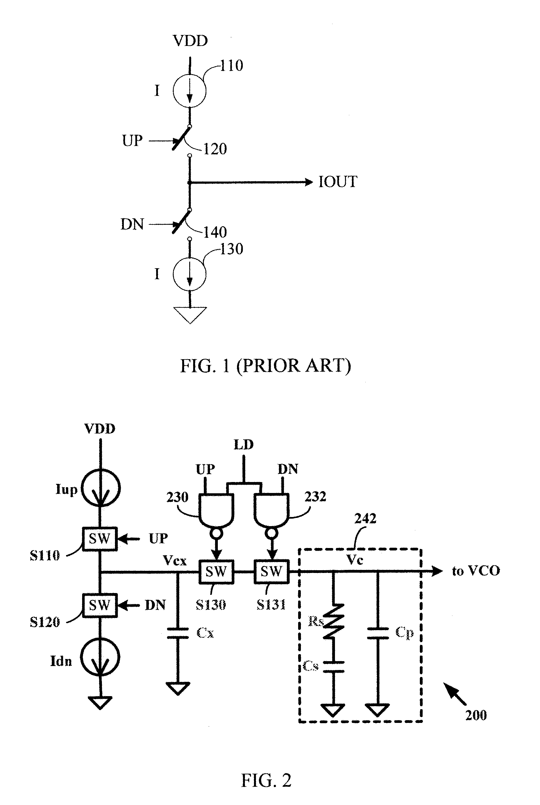
In practice, however, the prior art charge pump circuits shown in FIG. 1 are prone to problems due to circuit non-idealities.
These non-idealities will lead to performance degradation to the PLL.
First, the circuit complexity is high.
Second, the offset voltage of the operational amplifier will degrade the accuracy of the cancellation.
Third, it can at best alleviate the UP / DN current mismatch but still cannot solve the aforementioned problem of the noises induced due to the switching activities of switches.

Method used


Image

  • Charge pump circuit and method thereof
  • Charge pump circuit and method thereof
  • Charge pump circuit and method thereof

Examples


Embodiment Construction

[0018] In the present disclosure, numerous specific details are provided, such as examples of apparatus, circuits, components, and methods, to provide a thorough understanding of embodiments of the invention. Persons of ordinary skill in the art will recognize, however, that the invention can be practiced without one or more of the specific details. In other instances, well-known details are not shown or described to avoid obscuring aspects of the invention.

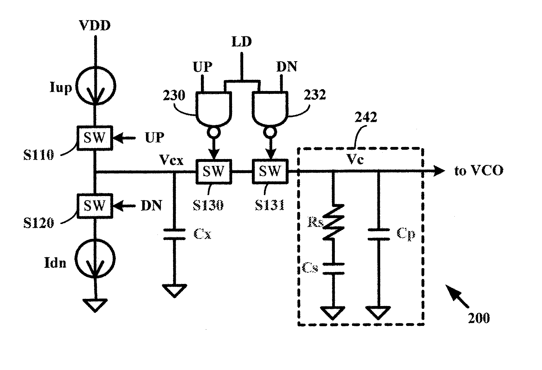
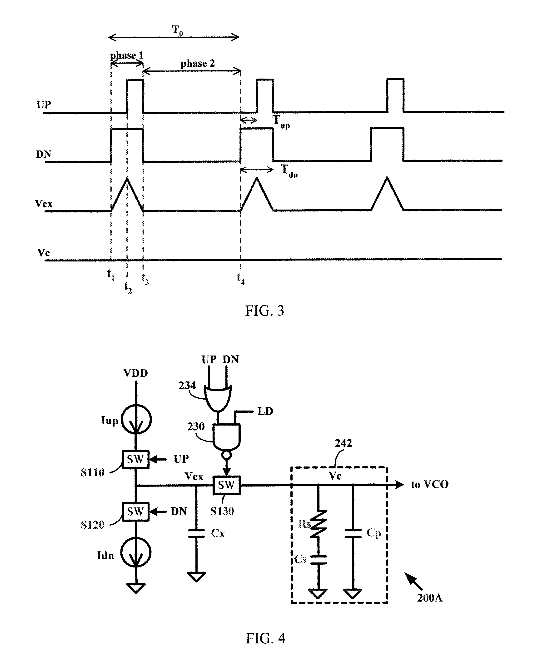
[0019]FIG. 2 depicts a schematic diagram of an embodiment of CP-LP (charge pump-loop filter) circuit 200 in accordance with the present invention. Here, CP-LP circuit 200 comprises a current source lup, a current sink Idn, and a first capacitor Cx. Iup is coupled to Cx through a first switch S110 controlled by the UP signal, while Idn is coupled to Cx through a second switch S120 controlled by the DN signal. CP-LP circuit 200 further comprises a loop filter 242. By way of example but not limitation, loop filter 242 comprises a s...


PUM


Abstract

A charge pump circuit capable of canceling current mismatch and suppressing clock feedthrough. The charge pump circuit comprises a current source enabled by a first logical signal, a current sink enabled by a second logical signal, an integrating capacitor coupled to both the current source and the current sink, and a switching device coupled between the integrating circuit and an output node. The switching device has two states. The switching device is set to a first state whenever a third logical signal is asserted and one of the first logical signal, the second logical signal, and a modulating signal is enabled. The switching device is set to a second state whenever the third logical signal is de-asserted, or none of the first logical signal, the second logical signal, and the modulating signal are asserted.

Description

BACKGROUND OF THE INVENTION [0001] 1. Field of the Invention [0002] The prevent invention relates to charge pump circuit, more particularly, to method and apparatus for canceling mismatch and suppressing clock feedthrough for charge pump circuit. [0003] 2. Description of Related Art [0004] A typical PLL (phase lock loop) comprises a PFD (phase / frequency detector), a charge pump circuit, a loop filter, and a VCO (voltage controlled oscillator). The PFD compares the phase of a reference clock with that of the output clock of the VCO. Usually two logical signals, said UP and DN signals are used by the PFD to represent the phase difference between the two clocks. Each time a phase comparison is made, an UP pulse and a DN pulse are generated. If the reference clock is leading the VCO output clock (in clock phase), the UP pulse is longer than the DN pulse. Otherwise, the DN pulse is longer than the UP pulse. The two logical signals are converted into a current signal using the charge pump...

Claims


Application Information

Patent Timeline
Patent Type & Authority Applications(United States)
IPC IPC(8): H03L7/06
CPCH03L7/0891H03L7/095H03L7/093H03L7/0896H03L7/0895
Inventor LEE, CHAO-CHENGLIU, REN-CHIEH
Owner REALTEK SEMICON CORP
Learn More