

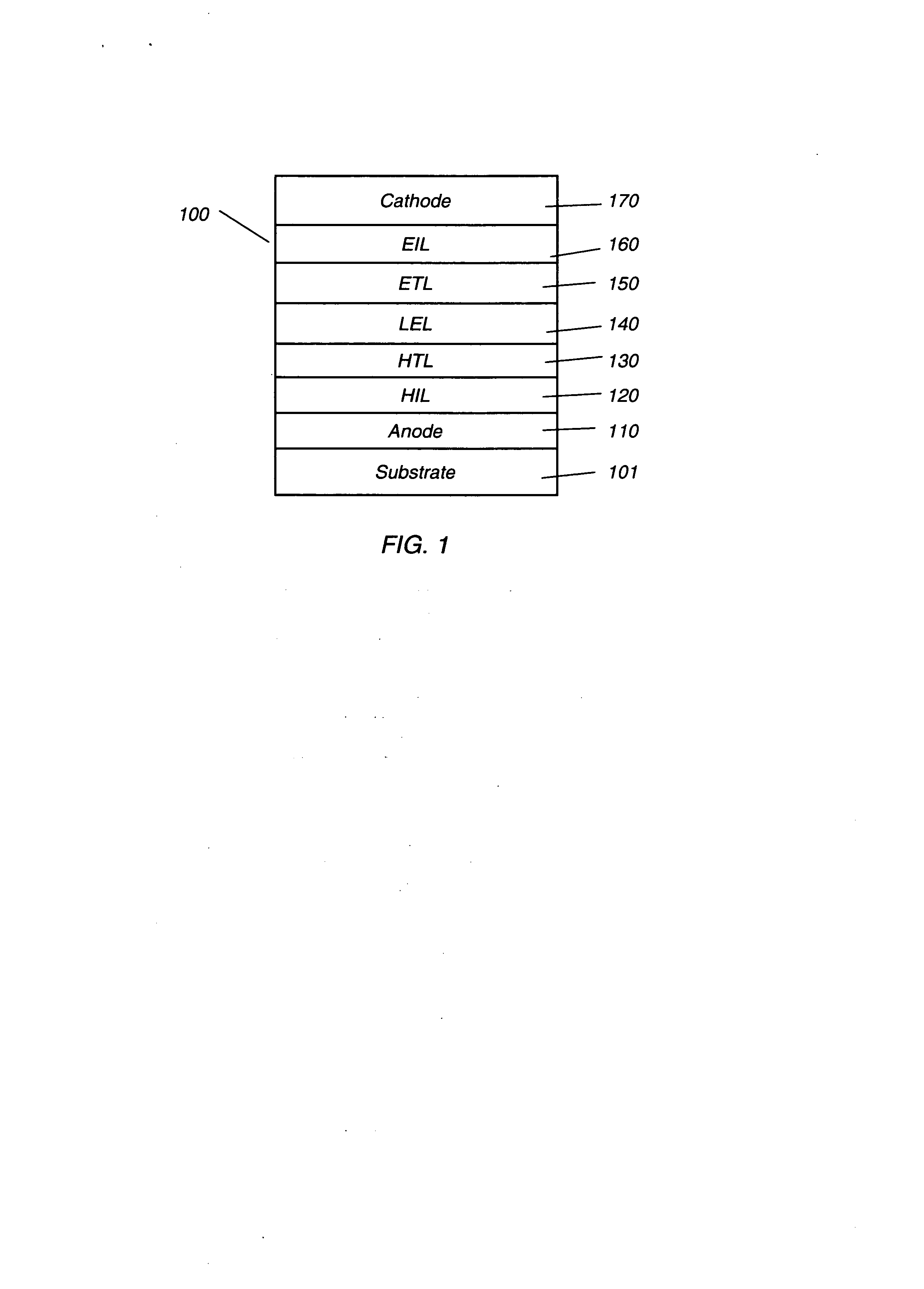
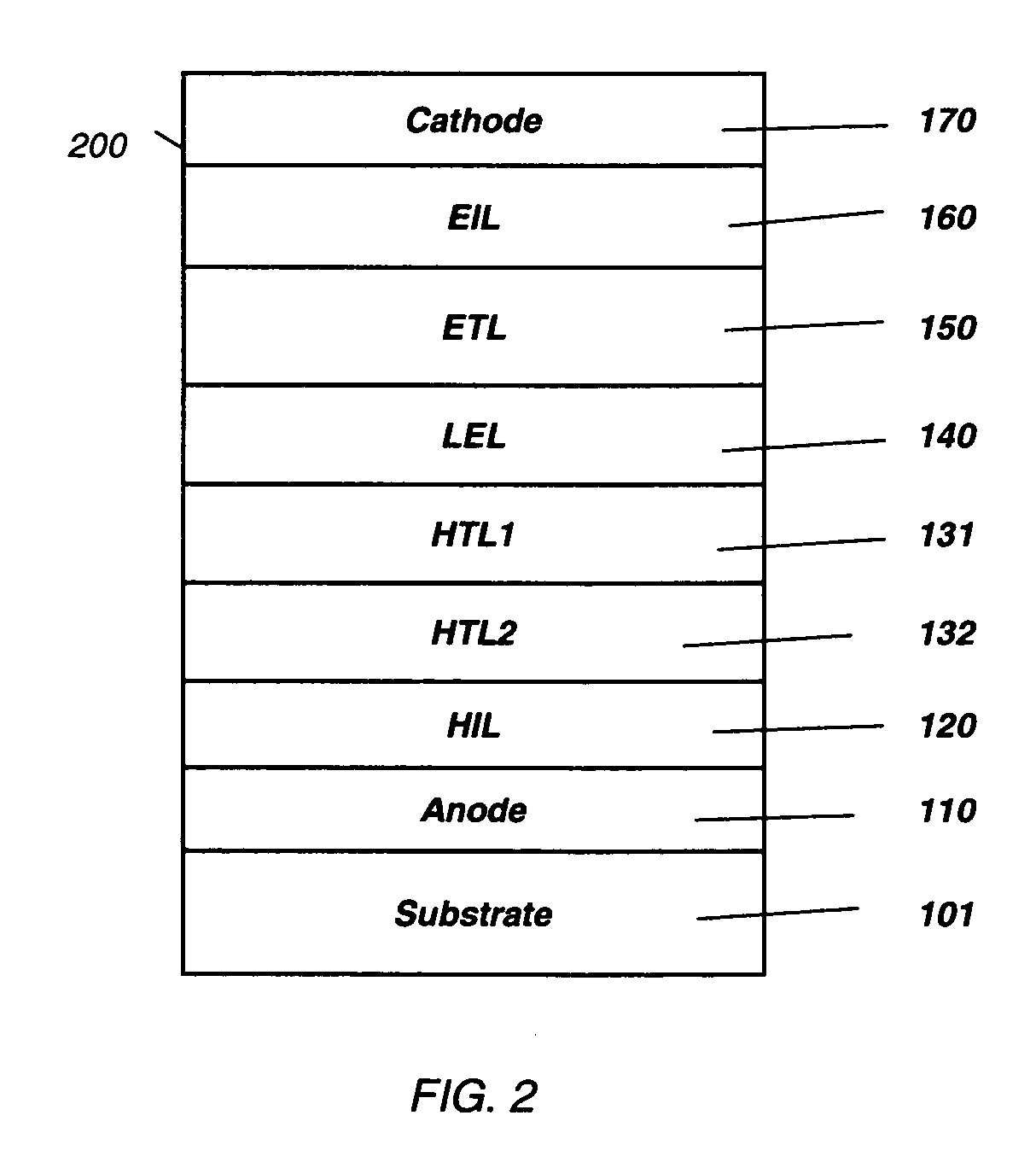
OLED device with improved efficiency and lifetime
a technology of luminance efficiency and lifetime, which is applied in the direction of discharge tube luminescnet screens, other domestic articles, natural mineral layered products, etc., can solve the problems of short lifetime, low efficiency poor stability of blue emitting devices, so as to reduce the change in the drive voltage during operation, reduce the change in the luminance efficiency, and reduce the effect of color chromaticity
- Summary
- Abstract
- Description
- Claims
- Application Information
AI Technical Summary
Benefits of technology
Problems solved by technology
Method used
Image

Examples
example 3
Invention
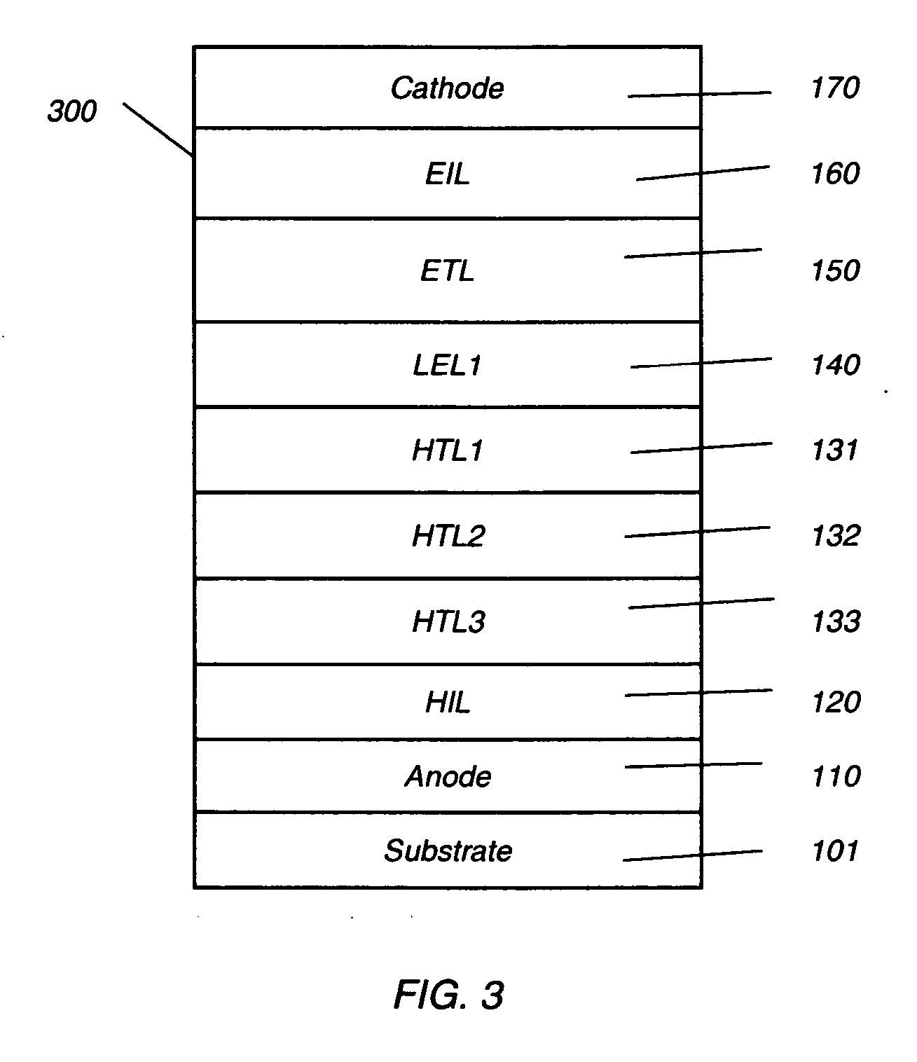
[0187] An inventive OLED device Example 3 of the invention was prepared following process. A clean glass substrate was vacuum-deposited with indium tin oxide (ITO) to form a transparent electrode 85 nm thick. The above-prepared ITO surface was treated with a plasma oxygen etch. The following layers were then deposited in the following sequence by evaporation from heated boats under a vacuum of approximately 10−6 Torr:
[0188] a) A 10 nm hexatriphenylene derivative (Formula Q1)
[0189] b) A 110 nm undoped hole-transporting layer of 4,4′-bis[N-(1-naphthyl)-N-phenylamino]biphenyl (NPB). This forms un-doped sublayer HTL3;
[0190] c) A 10 nm another hole transporting layer including 70% NPB (as host) and 30% antharacene derivative as one stabilizing dopant as shown in Formula AH3 and another stabilizing dopant 2% Rubrene derivative (Formula L50). This forms the hole transporting sublayer HTL2);
[0191] d) A 20 rim another hole transporting layer including 70% NPB (as host) and 30% ...
example 4
Invention
[0197] An inventive OLED device Example 4 of the invention was prepared following process. A clean glass substrate was vacuum-deposited with indium tin oxide (ITO) to form a transparent electrode 85 nm thick. The above-prepared ITO surface was treated with a plasma oxygen etch. The following layers were then deposited in the following sequence by evaporation from heated boats under a vacuum of approximately 10−6 Torr:
[0198] a) A 10 nm hexatriphenylene derivative (Formula Q1)
[0199] b) A 110 nm undoped hole-transporting layer of 4,4′-bis[N-(1-naphthyl)-N-phenylamino]biphenyl (NPB). This forms un-doped sublayer HTL3;
[0200] c) A 20 nm another hole transporting layer including 70% NPB (as host) and 30% antharacene derivative as one stabilizing dopant as shown in Formula AH3 and another stabilizing dopant 2% Rubrene derivative (Formula L50). This forms the hole transporting sublayer HTL2);
[0201] d) A 10 nm another hole transporting layer including 70% NPB (as host) and 30% a...
example 5
Invention
[0207] An OLED device Example 5 of the invention was prepared following process. A clean glass substrate was vacuum-deposited with indium tin oxide (ITO) to form a transparent electrode 85 nm thick. The above-prepared ITO surface was treated with a plasma oxygen etch. The following layers were then deposited in the following sequence by evaporation from heated boats under a vacuum of approximately 10−6 Torr:
[0208] a) A 10 nm hexatriphenylene derivative (Formula Q1)
[0209] b) A 110 nm undoped hole-transporting layer of 4,4′-bis[N-(1-naphthyl)-N-phenylamino]biphenyl (NPB). This forms un-doped sublayer HTL3;
[0210] c) A 20 nm second hole transporting layer including 70% NPB (as host) and 30% antharacene derivative as one stabilizing dopant as shown in Formula AH3 and another stabilizing dopant 1% perefluorenthene derivative (Formula Q10). This forms the hole transporting sublayer HTL2);
[0211] d) A 20 nm another hole transporting layer including 70% NPB (as host) and 30% ant...
PUM
| Property | Measurement | Unit |
|---|---|---|
| thickness | aaaaa | aaaaa |
| thickness | aaaaa | aaaaa |
| work function | aaaaa | aaaaa |
Abstract
Description
Claims
Application Information