Method to improve the step coverage and pattern loading for dielectric films

a dielectric film and pattern loading technology, applied in the direction of electric apparatus, semiconductor/solid-state device manufacturing, basic electric elements, etc., can solve the problems of difficult depositing barrier layers over features, difficult to achieve conformal deposition, and negatively affecting the drive current improvement of one devi

Active Publication Date: 2007-10-04
APPLIED MATERIALS INC
View PDF52 Cites 139 Cited by
  • Summary
  • Abstract
  • Description
  • Claims
  • Application Information

AI Technical Summary

Problems solved by technology

However, it is often difficult to achieve conformal deposition.
For example, it is difficult to deposit a barrier layer over a feature with few or no resulting surface defects or feature deformation.
The film thickness non-uniformity across the wafer can negatively impact the drive current improvement from one device to another.
Modulating the process parameters alone does not significantly improve the step coverage and pattern loading problems.
Deposition of conformal layers over gate stacks to provide layers that are subsequently etche

Method used


Image

  • Method to improve the step coverage and pattern loading for dielectric films
  • Method to improve the step coverage and pattern loading for dielectric films
  • Method to improve the step coverage and pattern loading for dielectric films

Examples


Embodiment Construction

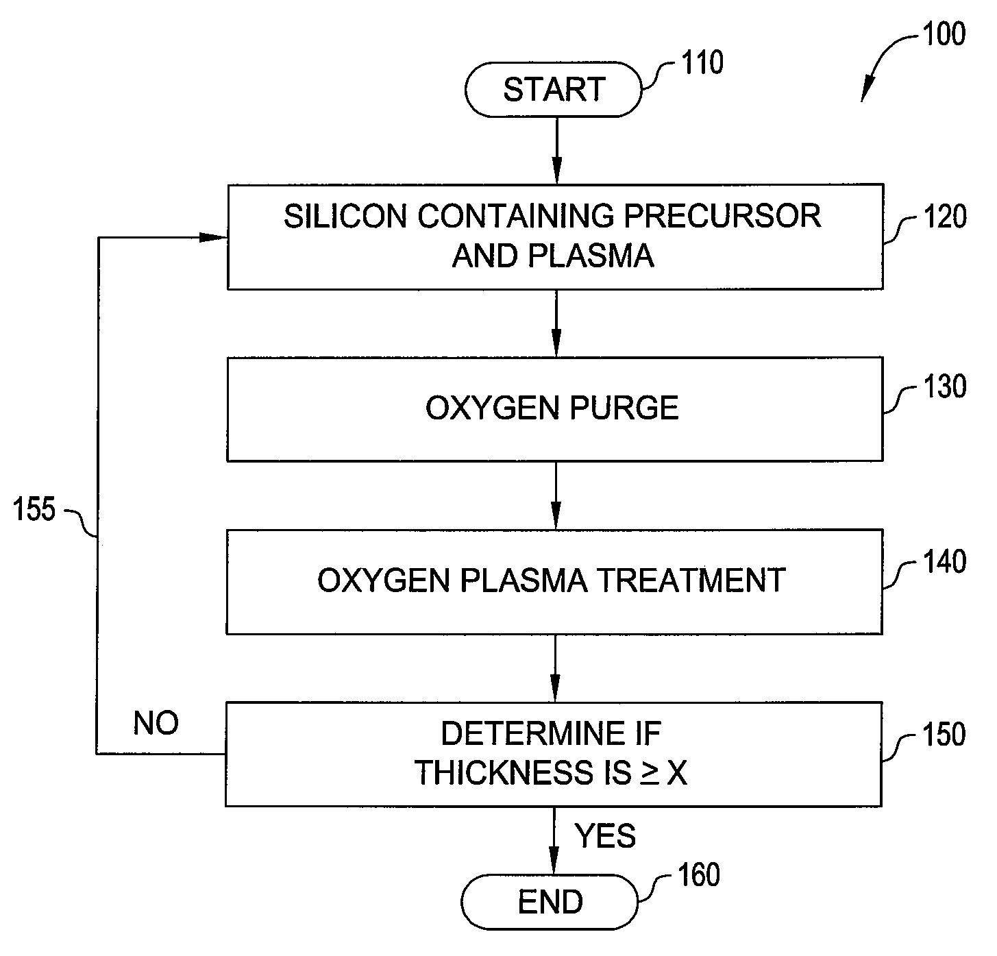
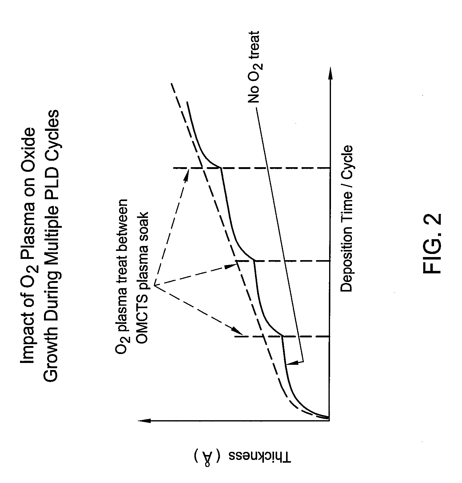
[0021]The present invention provides a method and apparatus for depositing a conformal dielectric film over a formed feature. The films that can benefit from this process include dielectric materials such as silicon oxide, silicon oxynitride, or silicon nitride. The films may be carbon doped, hydrogen doped, or contain some other chemical or element to tailor the dielectric properties. The layer may be carbon doped or nitrogen doped. Specifically, a combination of thin layers that have been individually deposited and plasma treated provide a more conformal film than a single thick dielectric layer. The chambers that are preferred for this process include the PRODUCER P3™ chamber, PRODUCER APF PECVD™ chamber, PRODUCER BLACK DIAMOND PECVD™ chamber, PRODUCER BLOK PECVD™ chamber, PRODUCER DARC PECVD™ chamber, PRODUCER HARP™ chamber, PRODUCER PECVD™ chamber, PRODUCER SACVD™ chamber, PRODUCER STRESS NITRIDE PECVD™ chamber, and PRODUCER TEOS FSG PECVD™ chamber, and each of these chambers i...


PUM


Abstract

A method of forming a layer on a substrate in a chamber, wherein the substrate has at least one formed feature across its surface, is provided. The method includes exposing the substrate to a silicon-containing precursor in the presence of a plasma to deposit a layer, treating the deposited layer with a plasma, and repeating the exposing and treating until a desired thickness of the layer is obtained. The plasma may be generated from an oxygen-containing gas.

Description

CROSS-REFERENCE TO RELATED APPLICATIONS[0001]This application claims benefit of U.S. provisional patent application Ser. No. 60 / 790,254, filed Apr. 7, 2006, and of U.S. provisional patent application Ser. No. 60 / 788,279, filed Mar. 31, 2006, both of which are herein incorporated by reference.BACKGROUND OF THE INVENTION[0002]1. Field of the Invention[0003]Embodiments of the present invention generally relate to a method and apparatus for semiconductor processing. Specifically, embodiments of the present invention relate to a method and apparatus for depositing a conformal dielectric film.[0004]2. Description of the Related Art[0005]Forming dielectric layers on a substrate by chemical reaction of gases is one of the primary steps in the fabrication of modern semiconductor devices. These deposition processes include chemical vapor deposition (CVD) as well as plasma enhanced chemical vapor deposition (PECVD), which uses plasma in combination with traditional CVD techniques.[0006]CVD and...

Claims


Application Information

Patent Timeline
IPC IPC(8): H01L21/469
CPCH01L21/02126H01L21/02164H01L21/0217H01L21/02274H01L21/76834H01L21/31612H01L21/31633H01L21/76829H01L21/76831H01L21/0228
Inventor BALSEANU, MIHAELASHEK, MEIYEEXIA, LI-QUNM'SAAD, HICHEM
Owner APPLIED MATERIALS INC
Why Eureka
Try Eureka