
Timing analyzing method and apparatus for semiconductor integrated circuit

a timing analysis and integrated circuit technology, applied in the field of timing analysis methods and apparatus for semiconductor integrated circuits, can solve the problems of inefficient iteration, burden on elimination of timing errors, and time-consuming timing analysis, and achieve the effect of reducing the time of timing analysis

Inactive Publication Date: 2007-10-04
SOCIONEXT INC
View PDF9 Cites 19 Cited by
  • Summary
  • Abstract
  • Description
  • Claims
  • Application Information

AI Technical Summary

Benefits of technology

[0033]The present invention addresses the reduction of timing analysis time. The present invention particularly addresses the completion of timing error elimination and layout correction within a short period of time.

Problems solved by technology

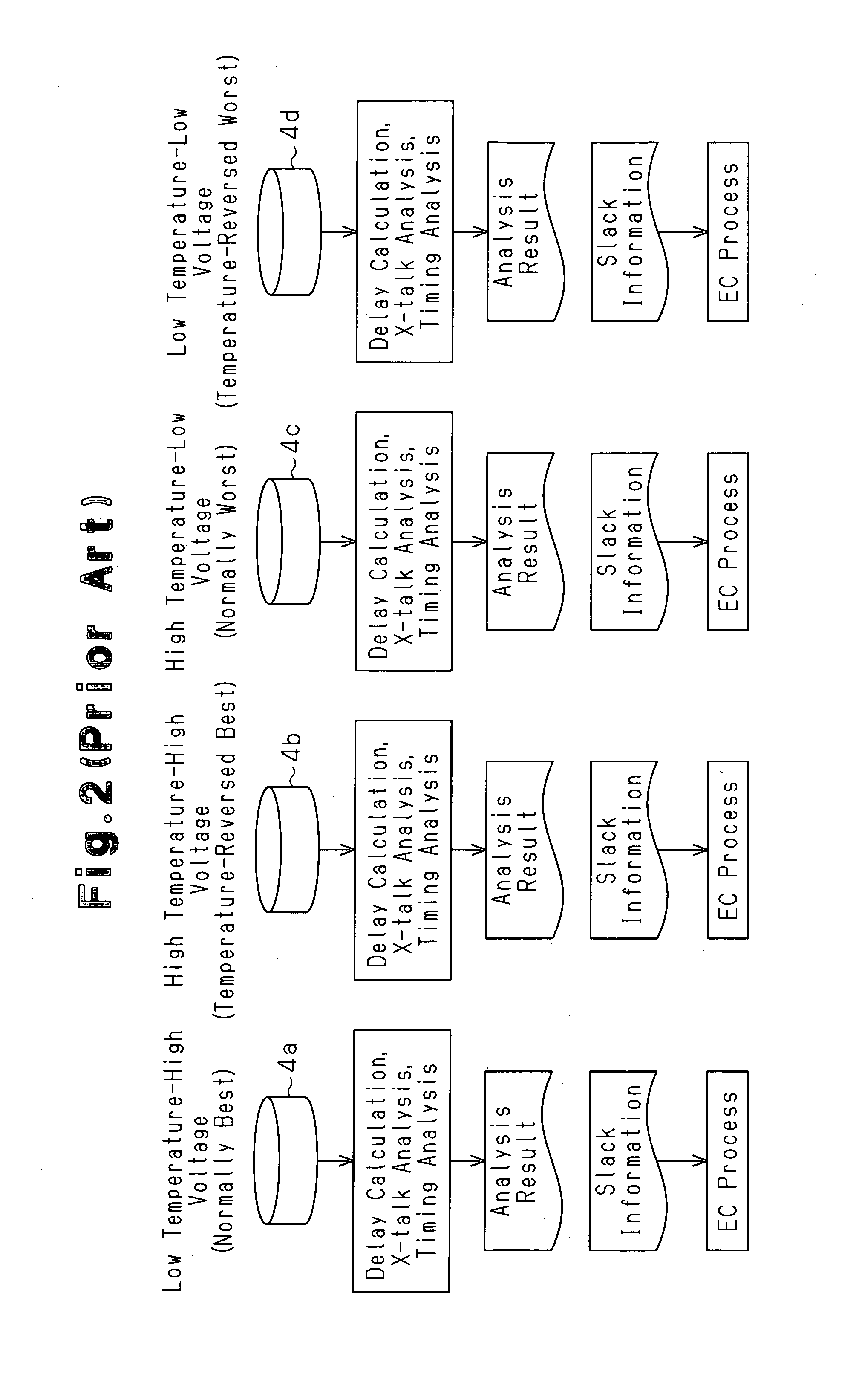
Further, when layout correction is performed to eliminate a timing error under a corner condition, a timing error occurs under other corner conditions.
In this manner, the timing analysis and layout correction under multi-corner conditions results in inefficient iteration.
Thus, the elimination of a timing error is burdensome.

Method used


Image

  • Timing analyzing method and apparatus for semiconductor integrated circuit
  • Timing analyzing method and apparatus for semiconductor integrated circuit
  • Timing analyzing method and apparatus for semiconductor integrated circuit

Examples


Embodiment Construction

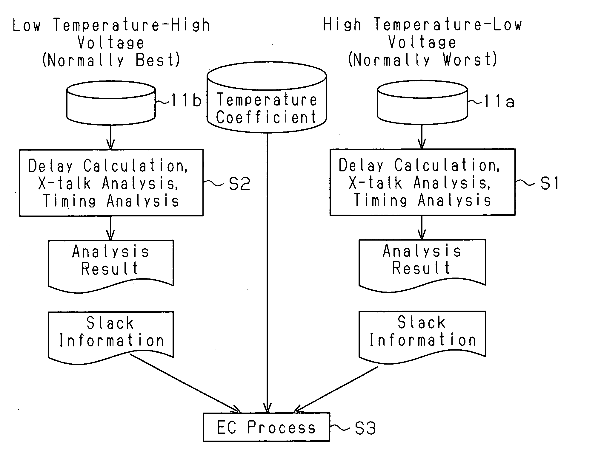
[0047]A preferred embodiment of the present invention will now be discussed with reference to the drawings. FIG. 4 is a flowchart illustrating a timing correction method and layout correction method according to the preferred embodiment. A library 11a stores delay information of gate delay for each cell and net delay under the worst-case corner condition, or the first corner condition, which is a combination of high temperature (upper limit temperature), low voltage (lower limit voltage), and slow process. A library 11b stores delay information of gate delay for each cell and net delay under the best-case corner condition, or the second corner condition, which is a combination of low temperature (lower limit temperature), high voltage (upper limit voltage), and fast process.

[0048]Under each corner condition, delay calculation, crosstalk (X-talk) analysis, and timing analysis are performed (steps S1 and S2). Based on the analysis results and the slack information, an EC process is pe...


PUM


Abstract

A method for analyzing timing in a semiconductor integrated circuit device with multi-corner conditions including a best-case corner condition and a worst-case corner condition. The best-case corner condition and the worst-case corner condition each include a temperature condition, with each temperature condition being a high temperature condition or a low temperature condition. The method includes storing in a temperature characteristic coefficient table a temperature characteristic coefficient for each of temperature-reversed corner conditions that are generated by selectively reversing the temperature conditions of the best-case corner condition and the worst-case corner condition, and performing timing analysis under said temperature-reversed corner conditions based on a gate delay and net delay calculated under the best-case corner condition and the worst-case corner condition and the temperature characteristic coefficient.

Description

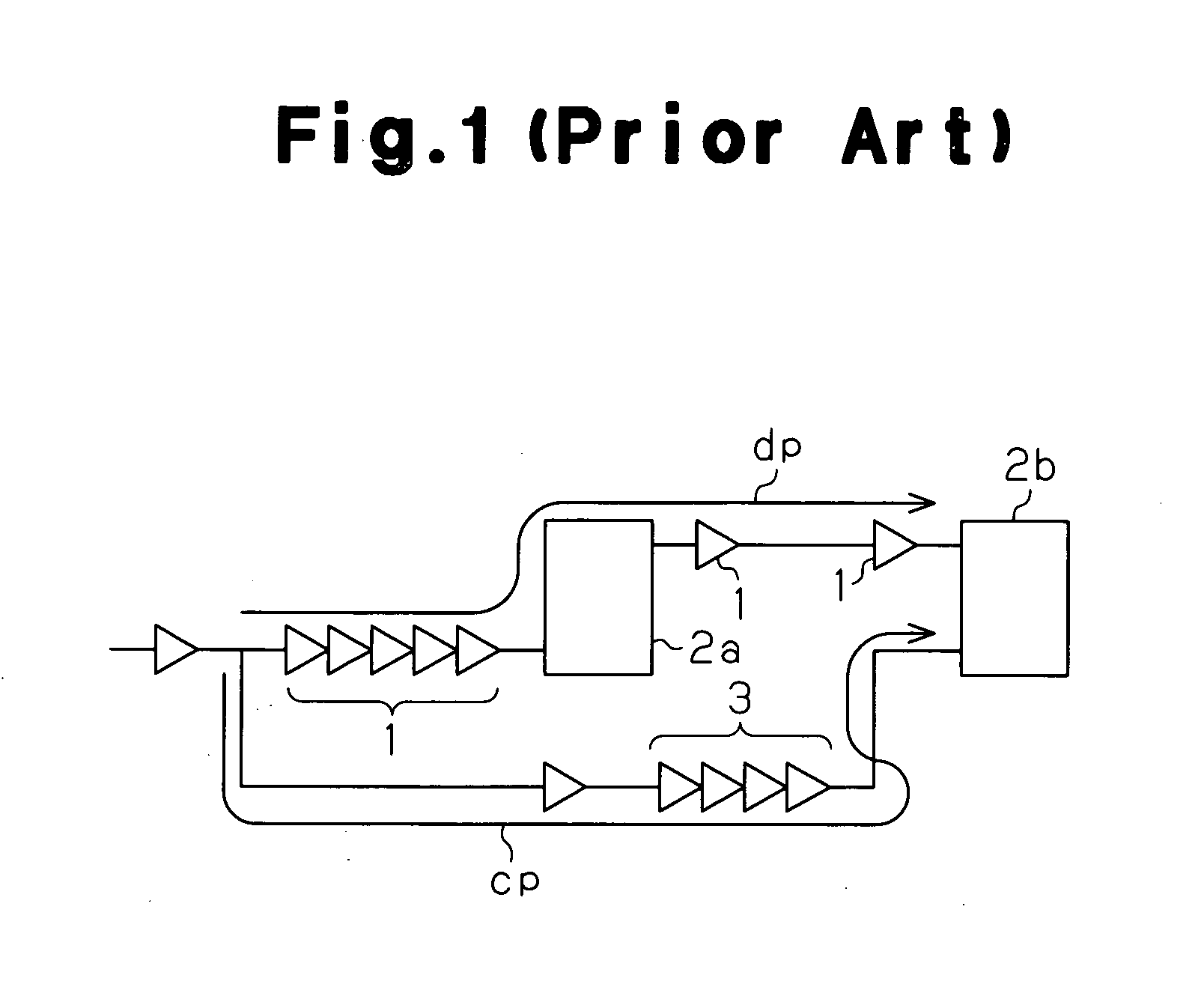
CROSS-REFERENCE TO RELATED APPLICATIONS[0001]This application is based upon and claims the benefit of priority from prior Japanese Patent Application No. 2006-099249, filed on Mar. 31, 2006, the entire contents of which are incorporated herein by reference.BACKGROUND OF THE INVENTION[0002]The present invention relates to a timing analyzing method and apparatus for a semiconductor integrated circuit.[0003]When a semiconductor integrated circuit is designed, timing analysis is performed taking into consideration gate delay, which is caused by cells forming the semiconductor integrated circuit, and net delay, which is caused by wiring (conductive paths) connecting the cells. The layout of the semiconductor integrated circuit is corrected based on the timing analysis results. The gate delay changes in accordance with the power supply voltage and the ambient temperature. The net delay changes in accordance with the ambient temperature. Thus, the timing analysis and layout correction must...

Claims


Application Information

Patent Timeline
IPC IPC(8): G06F17/50
CPCG06F2217/84G06F17/5031G06F30/3312G06F2119/12
Inventor YOSHIMURA, TERUMI
Owner SOCIONEXT INC
Learn More