Packaged system of semiconductor chips having a semiconductor interposer

a technology of interposer and semiconductor chip, which is applied in the direction of semiconductor devices, semiconductor/solid-state device details, electrical apparatus, etc., can solve the problems of solder joints, delamination of package parts, and significant failure rates, so as to reduce electrical resistance and inductance, improve speed and power capabilities

Active Publication Date: 2007-10-11
TEXAS INSTR INC
View PDF3 Cites 129 Cited by
  • Summary
  • Abstract
  • Description
  • Claims
  • Application Information

AI Technical Summary

Benefits of technology

[0005] Applicants further recognize the need to shrink semiconductor devices both in two and in three dimensions, especially for a device-stacking and package-on-package method for semiconductor devices as well as electronic systems. In Applicant's approach, the resulting system offers improved speed and power capabilities by minimizing electrical resistances and inductances, and replacing wire bonding with flip-chip assembly. An additional advantage of semiconductor interposers is the opportunity to build active electronic devices and even integrated circuits into the surface of the interposers.

Problems solved by technology

When the assembled devices are then used or tested under conditions, which impose wide swings of temperature or humidity on the packages, significant failure rates may appear, characterized by cracks, especially at the solder joints, and delamination of the package parts.
The reliability failure rates due to solder joint cracks or parts delamination, observed for these devices under conditions of temperature cycles and high humidity, are especially high.

Method used


Image

  • Packaged system of semiconductor chips having a semiconductor interposer
  • Packaged system of semiconductor chips having a semiconductor interposer
  • Packaged system of semiconductor chips having a semiconductor interposer

Examples


Embodiment Construction

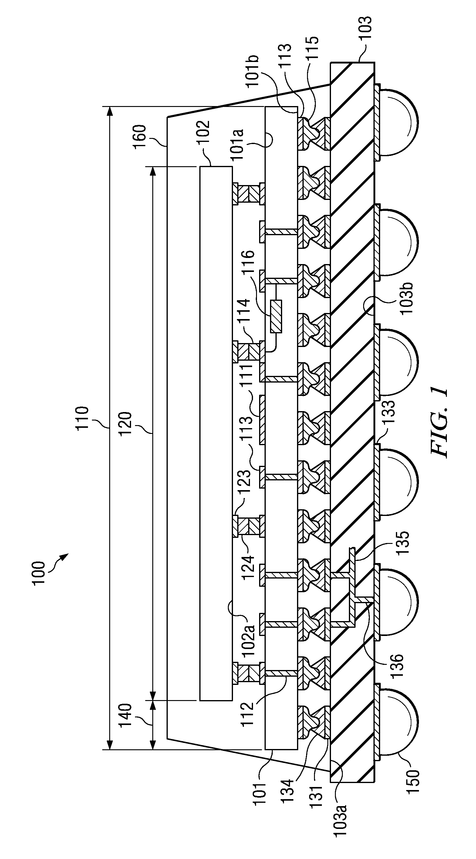
[0015]FIG. 1 illustrates a semiconductor system, generally designated 100, which includes an interposer 101 made of semiconductor material, a semiconductor chip 102, and a substrate 103 with an insulating base material. Although silicon is the preferred semiconductor material, the invention applies to any semiconductor material, such as germanium, silicon germanium, gallium arsenide, or other III-V and II-IV compounds used in device fabrication.

[0016] Interposer 101 has a certain dimension designated 110; in FIG. 1, the dimension is the interposer length; in other examples, it could be the interposer width. Furthermore, interposer has a first surface 101a and a second surface 101b. On the first surface 101a and on the second surface 101b are a plurality of conductive lines for electrical communication, patterned from metal layers such as copper or aluminum; while detailed lines are not shown in FIG. 1, some portions are indicated by 111. Some lines may be patterned as power buses (...


PUM


Abstract

A semiconductor system (200) of one or more semiconductor interposers (201) with a certain dimension (210), conductive vias (212) extending from the first to the second surface, with terminals and attached non-reflow metal studs (215) at the ends of the vias. A semiconducting interposer surface may include discrete electronic components or an integrated circuit. One or more semiconductor chips (202, 203) have a dimension (220, 230) narrower than the interposer dimension, and an active surface with terminals and non-reflow metal studs (224, 234). One chip is flip-attached to the first interposer surface, and another chip to the second interposer surface, so that the interposer dimension projects over the chip dimension. An insulating substrate (204) has terminals and reflow bodies (242) to connect to the studs of the projecting interposer.

Description

FIELD OF THE INVENTION [0001] The present invention is related in general to the field of semiconductor devices and processes, and more specifically to low profile, vertically integrated package-on-package semiconductor systems. DESCRIPTION OF THE RELATED ART [0002] When semiconductor chips are to be mounted on substrates or interposers to form today's semiconductor packages, the substrates and interposers are commonly made of plastic or ceramic materials. These materials are especially preferred when the chip assembly technique employs the flip-chip method using solder balls to create the electrical connections between the chips and the substrate / interposer. When the assembled devices are then used or tested under conditions, which impose wide swings of temperature or humidity on the packages, significant failure rates may appear, characterized by cracks, especially at the solder joints, and delamination of the package parts. [0003] Driven by the desire to reduce the board area nee...

Claims


Application Information

Patent Timeline
Patent Type & Authority Applications(United States)
IPC IPC(8): H01L23/02
CPCH01L21/4853H01L2225/1058H01L23/49811H01L23/5385H01L23/5389H01L24/16H01L25/0657H01L25/105H01L2224/16225H01L2225/06517H01L2225/0652H01L2225/06572H01L2924/01046H01L2924/01077H01L2924/01079H01L2924/14H01L2924/15311H01L2924/1532H01L2924/19011H01L2225/1023H01L23/3128
Inventor GERBER, MARK A.WACHTLER, KURT P.CASTRO, ABRAM M.
Owner TEXAS INSTR INC
Why Eureka
Try Eureka