

Substrate Treatment Method and Substrate Treatment Apparatus
a substrate treatment and substrate technology, applied in the direction of photomechanical treatment originals, machines/engines, instruments, etc., can solve the problems of inability to precisely control the amount of solvent vapor supplied to the substrate, the inability to form a contact hole with a desired diameter, and the inability to keep the concentration of solvent atmosphere in the container uniform
- Summary
- Abstract
- Description
- Claims
- Application Information
AI Technical Summary
Benefits of technology
Problems solved by technology
Method used
Image

Examples
Embodiment Construction
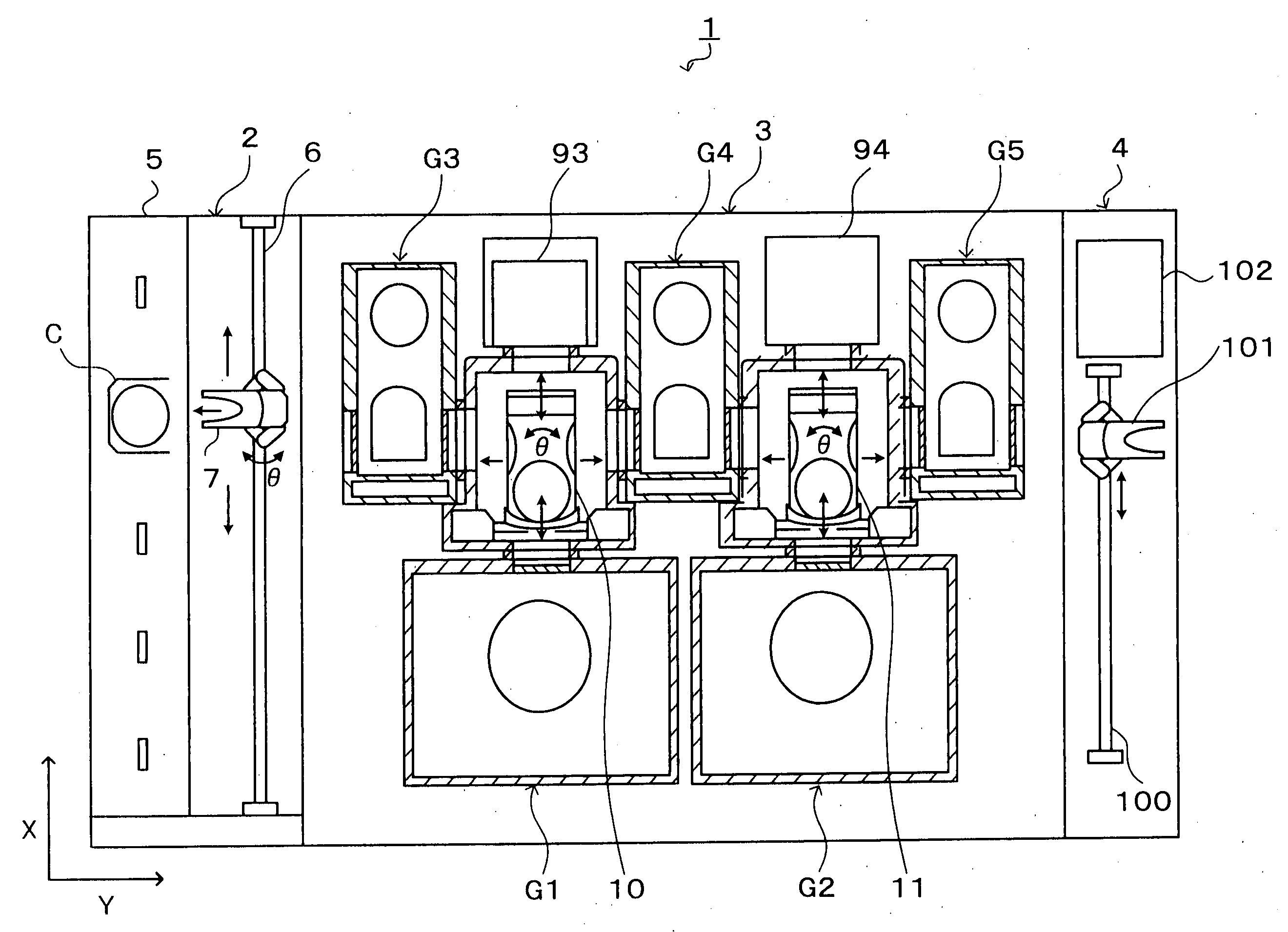
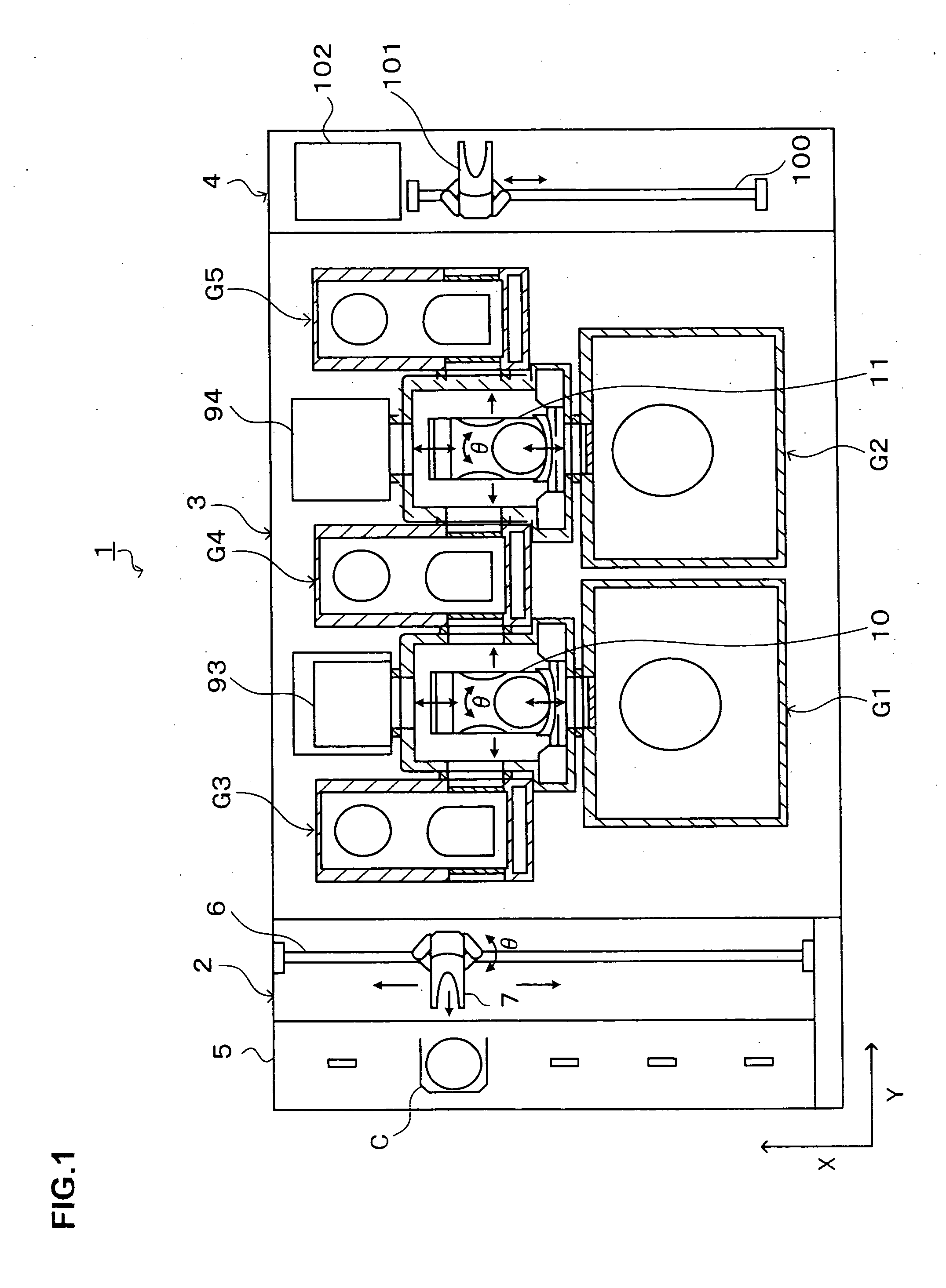
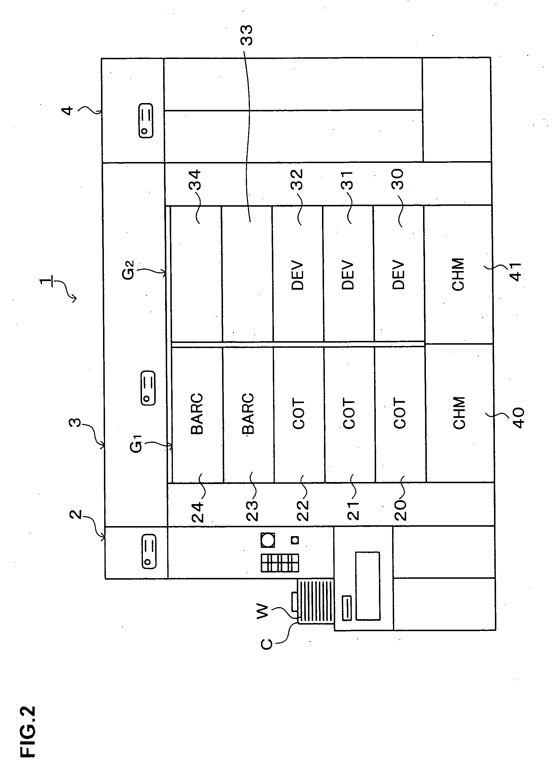
[0058] Hereinafter, preferred embodiments of the present invention will be described. FIG. 1 is a plan view showing the outline of a configuration of a coating and developing treatment system 1 in which a substrate treatment apparatus according to the present invention is installed, FIG. 2 is a front view of the coating and developing treatment system 1, and FIG. 3 is a rear view of the coating and developing treatment system 1.
[0059] The coating and developing treatment system 1 has, as shown in FIG. 1, a configuration in which, for example, a cassette station 2 for carrying, for example, 25 wafers W per cassette as a unit from / to the outside into / from the coating and developing treatment system 1 and carrying the wafers W into / out of a cassette C; a processing station 3 including a plurality of various kinds of processing and treatment units, which are multi-tiered, for performing predetermined processing or treatment in a manner of single wafer processing in the coating and deve...
PUM
| Property | Measurement | Unit |
|---|---|---|
| swelling | aaaaa | aaaaa |
| current | aaaaa | aaaaa |
| length | aaaaa | aaaaa |
Abstract
Description
Claims
Application Information