Sputtering apparatus

a technology of sputtering apparatus and monitor, which is applied in the direction of electrolysis components, vacuum evaporation coatings, coatings, etc., can solve the problems of reduced impaired control of film thickness, and limited flexibility in design within the film deposition chamber, so as to achieve enhanced flexibility in design and high-accuracy monitor control of film thickness

Inactive Publication Date: 2007-10-25
CANON KK
View PDF9 Cites 14 Cited by
  • Summary
  • Abstract
  • Description
  • Claims
  • Application Information

AI Technical Summary

Benefits of technology

[0010]The present invention provides a sputtering apparatus which enables highly accurate monitor control of a film thickness and allows enhanced flexibility in design.

Problems solved by technology

This is because a significant difference in the film deposition rate reduces the accuracy in control of the film thickness.
When the sensor is installed as disclosed in Japanese Patent Laid-Open No. 08(1996)-325725, there is concern that control of film thickness is impaired due to such a difference in the film deposition rate.
When the film-thickness measuring sensor is placed near the substrate such as on the side or on the back of the substrate as disclosed in Japanese Patent Laid-Open No. 08(1996)-325725, flexibility in design within the film deposition chamber is limited.
Those sensor-associated structures occupy a large volume of the film deposition chamber to limit the flexibility in design within the film deposition chamber.
This results in limited flexibility in the area and method of placement of the substrate within the film deposition chamber.

Method used


Image

  • Sputtering apparatus
  • Sputtering apparatus
  • Sputtering apparatus

Examples


embodiment 1

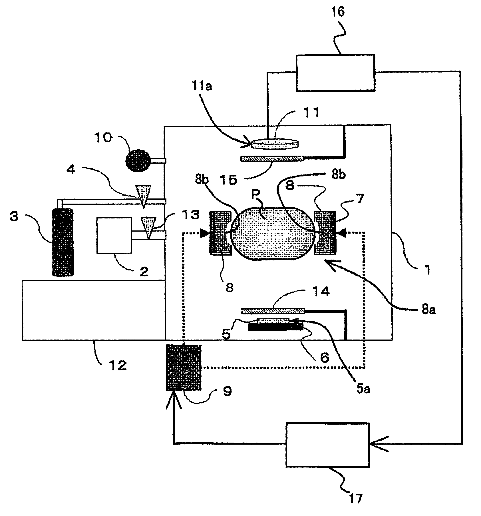
[0028]FIG. 1 shows the structure of a sputtering apparatus which is Embodiment 1 of the present invention. The sputtering apparatus of Embodiment 1 includes a film deposition chamber (vacuum chamber) 1 in which a film is deposited, a vacuum pump 2 which performs exhaust from the film deposition chamber 1, and a gas cylinder 3 which introduces, into the film deposition chamber 1, a gas for producing plasma discharge within the film deposition chamber 1. Gasses for use in the sputtering apparatus include an inert gas such as Ar (argon) and He (helium), and a mixture such as a mixture of an inert gas and O2 (oxygen) or N2 (nitrogen).

[0029]An exhaust valve 13 is provided for controlling the volume of exhaust between the film deposition chamber 1 and the vacuum pump 2. A gas introducing valve 4 is provided for controlling the supply of the gas between the film deposition chamber 1 and the gas cylinder 3.

[0030]The sputtering apparatus also includes a load lock chamber 12 for carrying a su...

embodiment 2

[0078]FIG. 5 shows the positional relationship between a particle emission area 28a, a substrate placement area 5a, and a sensor placement area 11a in the structure of a sputtering apparatus which is Embodiment 2 of the present invention. The three areas 5a, 28a, and 11a are shown by chain double dashed lines. FIG. 5 shows a substrate 5, a target 28, and a sensor 11 placed in the three areas 5a, 28a, and 11a, respectively. In Embodiment 2, components identical to those in Embodiment 1 are designated with the same reference numerals as those in Embodiment 1. This applies to Embodiments 3 and 4, later described.

[0079]The sputtering apparatus of Embodiment 2 is of a parallel-plate type (opposed type) in which the target 28 in a planar shape is placed in the particle emission area 28a such that a sputtering surface 28b faces the substrate 5 and the sensor 11. In FIG. 5, O represents the center of the particle emission area 28a, and L1 represents the center line of the particle emission ...

embodiment 3

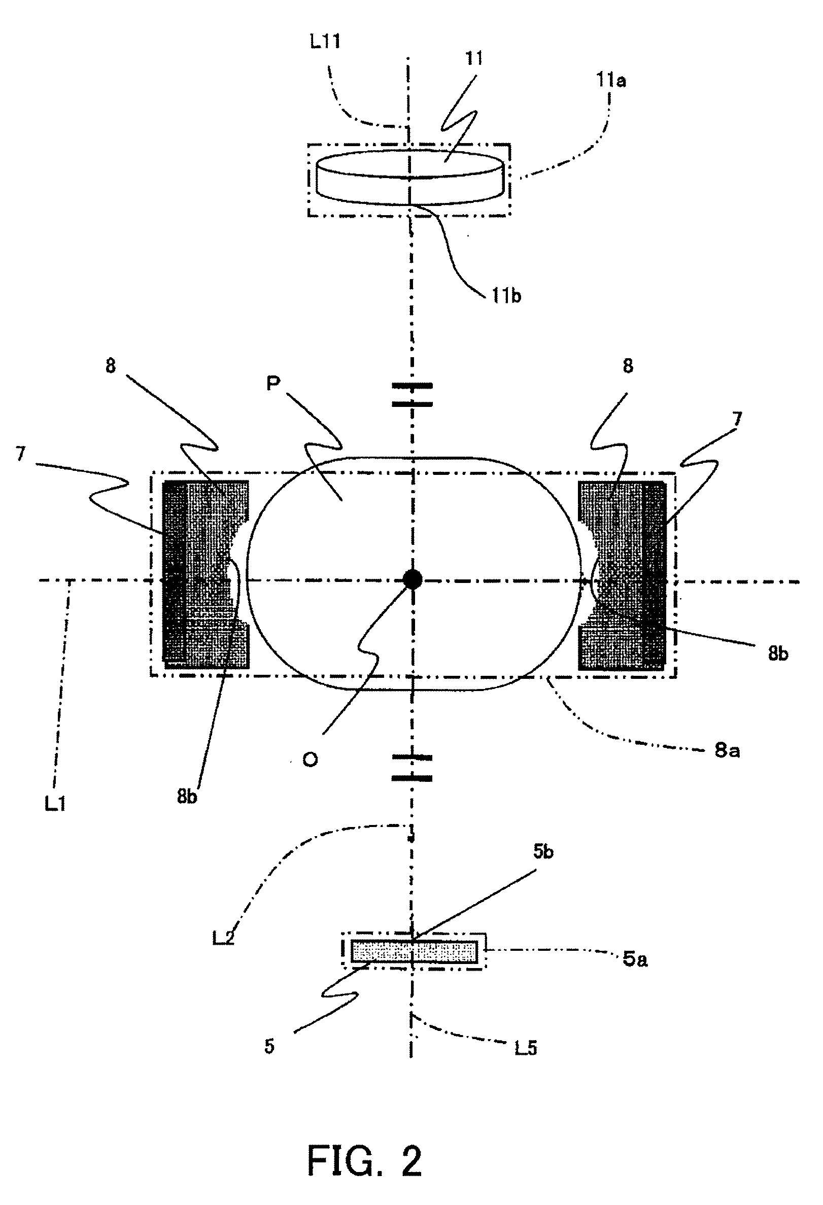
[0093]FIG. 6 shows the positional relationship between a particle emission area 8a, a substrate placement area 5a, and a sensor placement area 11a in the structure of a sputtering apparatus which is Embodiment 3 of the present invention. The three areas 5a, 8a, and 11a are shown by chain double dashed lines. FIG. 6 shows a substrate 5, targets 8, and a sensor 11 placed in the three areas 5a, 8a, and 11a, respectively.

[0094]The sputtering apparatus of Embodiment 3 is of the off-axis or opposed-target type in which the two planar targets 8 are placed such that their sputtering surfaces 8b are opposite to each other, similarly to Embodiment 1.

[0095]In FIG. 6, L1 and L2 represent a center line in the vertical direction and a center line in the horizontal direction, respectively, of the particle emission area 8a as described in Embodiment 1.

[0096]In the sputtering apparatus of Embodiment 3, the substrate placement area 5a (that is, the substrate 5) and the sensor placement area 11a (that...


PUM

PropertyMeasurementUnit
thicknessaaaaaaaaaa
areaaaaaaaaaaa
particle emission areaaaaaaaaaaa

Abstract

A sputtering apparatus is disclosed which enables highly accurate monitor control of a film thickness and allows enhanced flexibility in design. The apparatus includes a substrate placement area in which a substrate is placed, a particle emission area in which a target is placed and sputter particles from the target are emitted, and a sensor placement area in which a sensor is placed for measuring a thickness of a film formed on the substrate. The substrate placement area and the sensor placement area are provided in a positional relationship having symmetry with respect to a center line of the particle emission area.

Description

BACKGROUND OF THE INVENTION[0001]The present invention relates to a sputtering apparatus for forming (depositing) a film on an object, and more particularly, to a sputtering apparatus which forms a film having a thickness controlled accurately by using a sensor for measuring a film thickness.[0002]In sputtering apparatuses, a target serving as a material of a thin film and an object (hereinafter referred to as a substrate) on which the thin film should be deposited are placed in a film deposition chamber, and sputtering is performed through electrical discharge on a surface (sputtering surface) of the target to be sputtered, thereby producing the thin film made of metal or compound material on the surface (film deposition surface) of the substrate on which the film should be deposited.[0003]Such sputtering apparatuses include opposed-type sputtering apparatuses in which a sputtering surface of a target is opposed to a film deposition surface of a substrate on which a film should be ...

Claims


Application Information

Patent Timeline
Patent Type & Authority Applications(United States)
IPC IPC(8): C23C14/00
CPCC23C14/3464H01J37/34H01J37/32935C23C14/546
Inventor TOKIMITSU, TAKUMI
Owner CANON KK
Why Eureka
Try Eureka