An atomic layer deposition technique for growing v x c nanomaterials approach

An atomic layer deposition, nanomaterial technology, applied in nanotechnology, nanotechnology, metal material coating process, etc., can solve the problem of corrosion of hydrogen halide, etc., and achieve the effect of low resistivity and excellent compatibility

Active Publication Date: 2021-10-22
JIANGNAN UNIV
View PDF5 Cites 0 Cited by
  • Summary
  • Abstract
  • Description
  • Claims
  • Application Information

AI Technical Summary

Problems solved by technology

[0005] The prior art WO 01 / 29280A1 discloses a method for preparing vanadium carbide materials using vanadium halides as metal sources, but metal halides will produce considerable hydrogen halides that corrode ALD equipment during the ALD deposition process, so they are gradually abandoned

Method used


Image

  • An atomic layer deposition technique for growing v  <sub>x</sub> c nanomaterials approach
  • An atomic layer deposition technique for growing v  <sub>x</sub> c nanomaterials approach
  • An atomic layer deposition technique for growing v  <sub>x</sub> c nanomaterials approach

Examples


Embodiment 1

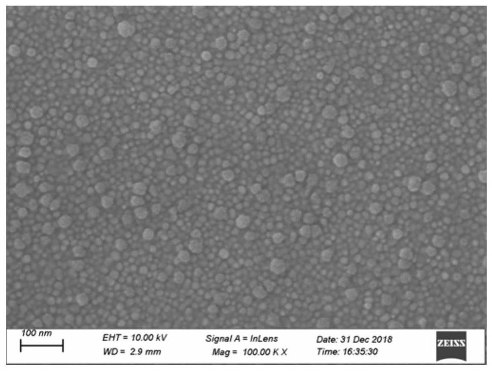
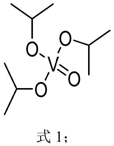
[0044] Using triisopropoxyvanadium oxide as V source and tetrahydrofuran as carbon source, V x The method for C nanomaterials comprises the following steps: taking SiO 2 As the substrate, the substrate is placed in the reaction chamber, the deposition temperature is 260°C, the triisopropoxyvanadium oxide is heated to a temperature of 70°C to vaporize it, and high-purity nitrogen is used as the carrier gas to pass into the gas phase Triisopropoxy vanadium oxide, the carrier gas flow is 10sccm, and the pulse time is 4s; After completing a pulse of step (1), use high-purity nitrogen to purge, and the purge time is 60s; carbon source tetrahydrofuran is heated to a temperature of 45°C, make it gasified, use high-purity nitrogen as the carrier gas, the carrier gas flow rate is 20sccm, pass tetrahydrofuran into the reaction chamber in pulse form, the pulse time is 1s, tetrahydrofuran reacts with the V source deposited on the substrate, get monoatomic layer V x The substrate of C na...

Embodiment 2

[0047] Using triisopropoxyvanadium oxide as the V source and diethyl ether as the carbon source, V x The method of C nanometer material, comprises the following steps:

[0048] Using silicon as the substrate, place the substrate in the reaction chamber, the deposition temperature is 280°C, heat the triisopropoxyvanadium oxide to a temperature of 75°C to vaporize it, and use high-purity nitrogen as the carrier gas to pass Into the gas phase vanadium triisopropoxide, the flow rate of the carrier gas is 20sccm, and the pulse time is 6s; after one pulse is completed, use high-purity nitrogen to purge, and the purge time is 65s; the carbon source ether is heated at 28°C to make it With high-purity nitrogen as the carrier gas, the flow rate of the carrier gas is 200 sccm, and ether is passed into in pulse form, and the pulse time is 3s; (4) after completing a pulse, high-purity nitrogen is used for purging, and the purging time is 12s, namely Complete one ALD cycle.

[0049] Repea...

Embodiment 3

[0051] Using triisopropoxyvanadium oxide as the V source and propyl ether as the carbon source, V x The method for C nanomaterials comprises the following steps: using silicon nitride as a substrate, placing the substrate in a reaction chamber, the deposition temperature is 300°C, and the heating temperature of triisopropoxyvanadium oxide is 80°C, making it gas Chemical, using high-purity nitrogen as the carrier gas, passing through the gaseous phase triisopropoxyvanadium oxide, the carrier gas flow rate is 30sccm, and the pulse time is 7s; after completing a pulse, use high-purity nitrogen to purge, and the purge time is 56s; The carbon source propyl ether is heated at 33°C to vaporize it. High-purity nitrogen is used as the carrier gas, and the carrier gas flow rate is 120 sccm. The propyl ether is passed into the pulse form, and the pulse time is 4s; after a pulse is completed, high-purity nitrogen is used. Purging is carried out, and the purging time is 36s, that is, one A...


PUM

PropertyMeasurementUnit
thicknessaaaaaaaaaa
electrical resistivityaaaaaaaaaa
thicknessaaaaaaaaaa

Abstract

The invention discloses an atomic layer deposition technique for growing V x The method of C nanomaterials belongs to the field of nanomaterials. Under vacuum conditions, the vaporized triisopropoxyvanadium oxide is introduced into the reaction chamber in a pulse form for deposition to obtain a substrate deposited with a V source. After sweeping, the gas-phase carbon source is introduced in a pulse form, and a single-atom reaction is performed with the V source deposited on the substrate to obtain a single-atom layer of V x C nanomaterials, purging again, and then repeating the above steps 1 to 2000 times, can be prepared by atomic layer deposition technology growth V x C nanomaterials, wherein the carbon source is one of ether, propyl ether, butyl ether, or tetrahydrofuran. The present invention adopts the combination of triisopropoxy vanadium oxide and carbon source, and further applies it in atomic layer deposition technology, so that it can be deposited on a nanoscale substrate to form V-containing x C deposition layer.

Description

technical field [0001] The present invention relates to a kind of atomic layer deposition technique growth V x A method for nanomaterials belongs to the field of nanomaterials. Background technique [0002] With the consumption of energy, people's demand for clean and sustainable energy is increasing, which further promotes the development of hydrogen energy. As an ideal and efficient hydrogen production technology, electrolysis of water technology has attracted extensive attention from researchers; However, the current challenge of this technology is the need to find suitable electrocatalysts. At present, noble metal catalysts (Pt-based) have good hydrogen evolution performance, but the disadvantages of low content on the earth's crust and high cost limit their wide application. Therefore, it is of great research significance to develop efficient and inexpensive hydrogen evolution electrocatalysts that can replace Pt-based materials. In recent years, researchers have rep...

Claims


Application Information

Patent Timeline
Patent Type & Authority Patents(China)
IPC IPC(8): C23C16/455C23C16/32C23C16/52C25B1/04C25B11/052C25B11/075B82Y30/00B82Y40/00
CPCB82Y30/00B82Y40/00C23C16/32C23C16/45527C23C16/52C25B1/04Y02E60/36
Inventor 杜立永何冬梅丁玉强
Owner JIANGNAN UNIV
Why Eureka
Try Eureka