Nitride semiconductor light-emitting device and method of manufacturing nitride semiconductor light-emitting device

a technology of nitride semiconductor and light-emitting device, which is applied in the direction of semiconductor lasers, solid-state devices, lasers, etc., can solve the problems of insufficient improvement of conventionally difficult to achieve higher reflectance at the light-emitting facet of the cavity, so as to achieve a lower threshold value and reduce the effect of mirror loss

Active Publication Date: 2007-10-25
SHARP FUKUYAMA LASER CO LTD
View PDF32 Cites 34 Cited by
  • Summary
  • Abstract
  • Description
  • Claims
  • Application Information

AI Technical Summary

Benefits of technology

[0004]Here, in the nitride semiconductor laser device, the threshold value can be lowered by raising the reflectance at the light-emitting facet of the cavity with respect to the laser beams to thereby lower mirror loss. Meanwhile, as the light-emitting facet of the cavity of the nitride semiconductor laser device may be broken due to COD (Catastrophic Optical Damage), a COD level (optical output at the time when the light-emitting facet of the cavity is broken due to COD) should be raised.

Problems solved by technology

If a single layer of a silicon oxide film, an aluminum oxide film, a titanium oxide film, a tantalum oxide film, a zinc oxide film, or the like is formed as an AR coating film on the light-emitting facet of the cavity of the nitride semiconductor laser device, however, improvement in the reflectance at the light-emitting facet of the cavity has not been sufficient.
Moreover, as optical density at the light-emitting facet of the cavity is increased when the reflectance at the light-emitting facet of the cavity is higher, it has been conventionally difficult to achieve higher reflectance at the light-emitting facet of the cavity while maintaining high COD level.

Method used


Image

  • Nitride semiconductor light-emitting device and method of manufacturing nitride semiconductor light-emitting device
  • Nitride semiconductor light-emitting device and method of manufacturing nitride semiconductor light-emitting device
  • Nitride semiconductor light-emitting device and method of manufacturing nitride semiconductor light-emitting device

Examples


Embodiment Construction

[0029]An embodiment of the present invention will be described hereinafter. In the drawings of the present invention, it is noted that the same reference characters represent the same or corresponding elements.

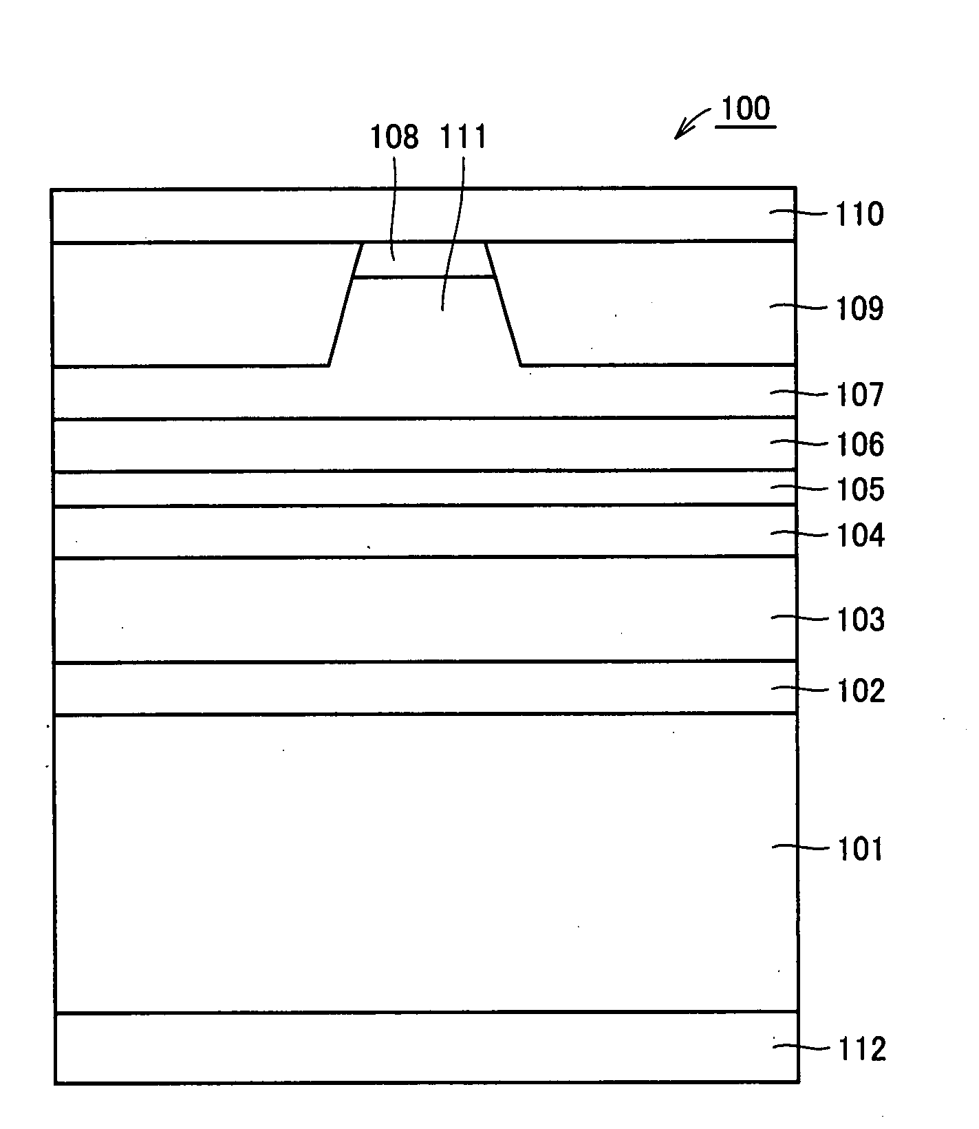
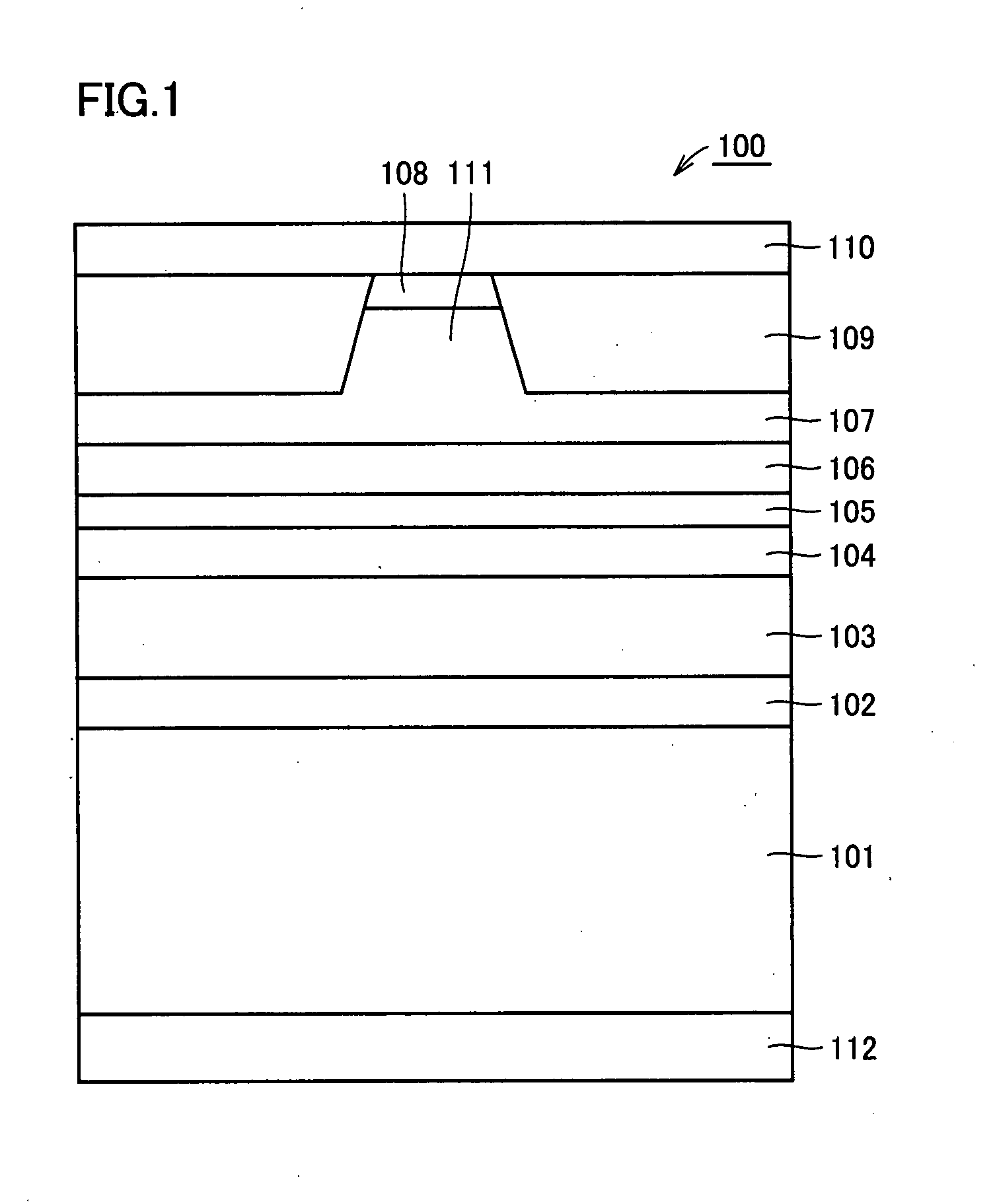
[0030]FIG. 1 is a schematic cross-sectional view of a preferred exemplary nitride semiconductor laser device representing a nitride semiconductor light-emitting device of the present invention. Here, a nitride semiconductor laser device 100 is structured such that, through epitaxial growth, an n-type buffer layer 102 composed of n-type GaN having a thickness of 0.2 cm, an n-type clad layer 103 composed of n-type Al0.06Ga0.94N having a thickness of 2.3 cm, an n-type guide layer 104 composed of n-type GaN having a thickness of 0.02 cm, a multiple quantum well active layer 105 constituted of a multiple quantum well layer composed of InGaN having a thickness of 4 nm and GaN having a thickness of 8 nm and a protection layer composed of GaN having a thickness of 70 nm, a p-type curr...


PUM

PropertyMeasurementUnit
reflectanceaaaaaaaaaa

Abstract

A nitride semiconductor light-emitting device including a coating film and a reflectance control film successively formed on a light-emitting portion, in which the light-emitting portion is formed of a nitride semiconductor, the coating film is formed of an aluminum oxynitride film or an aluminum nitride film, and the reflectance control film is formed of an oxide film, as well as a method of manufacturing the nitride semiconductor light-emitting device are provided.

Description

[0001]This nonprovisional application is based on Japanese Patent Applications Nos. 2006-119500 and 2007-077362 filed with the Japan Patent Office on Apr. 24, 2006 and Mar. 23, 2007, respectively, the entire contents of which are hereby incorporated by reference.FIELD OF THE INVENTION[0002]The present invention relates to a nitride semiconductor light-emitting device and a method of manufacturing a nitride semiconductor light-emitting device.DESCRIPTION OF THE BACKGROUND ART[0003]In a nitride semiconductor laser device representing nitride semiconductor light-emitting devices, in order to control reflectance at a facet of a cavity with respect to laser beams, an AR (Anti-Reflectance) coating film for attaining the reflectance of approximately 10% at the facet of the cavity with respect to the laser beams may be formed on a light-emitting facet of the cavity that should serve as a light-emitting portion of the nitride semiconductor laser device, and an HR (High-Reflectance) coating f...

Claims


Application Information

Patent Timeline
Patent Type & Authority Applications(United States)
IPC IPC(8): H01L33/00H01S5/028
CPCB82Y20/00H01S5/0014H01S5/34333H01S5/221H01S5/2231H01S5/028
Inventor KAMIKAWA, TAKESHIKAWAGUCHI, YOSHINOBU
Owner SHARP FUKUYAMA LASER CO LTD
Why Eureka
Try Eureka