Solid-state image sensing device and image sensing device

a sensing device and solid-state technology, applied in the direction of radioation control devices, television system scanning details, television systems, etc., can solve the problem of difficult to completely stabilize the current ids flowing into the amplifier, and achieve the effect of effectively adjusting the resistance value and suppressing the occurrence of streaking

Active Publication Date: 2007-10-25
PANASONIC SEMICON SOLUTIONS CO LTD
View PDF1 Cites 6 Cited by
  • Summary
  • Abstract
  • Description
  • Claims
  • Application Information

AI Technical Summary

Benefits of technology

[0023]As described above, this structure allows suppression of the occurrence of streaking in an output image. Especially since influence of a resistance provided on the ground side of the amplifier is greater than influence of a resistance provided on the power supply side, the above-mentioned structure enables to more effectively adjust the ratio of the resistance value on the power supply side of the amplifier to the resistance value on the ground side.

Problems solved by technology

However, the conventional solid-state image sensing device disclosed in the Japanese Laid-Open Patent Publication No. 2005-252529 has still difficulty in completely stabilizing the current Ids flowing into the amplifier.

Method used


Image

  • Solid-state image sensing device and image sensing device
  • Solid-state image sensing device and image sensing device
  • Solid-state image sensing device and image sensing device

Examples


embodiment 1

Variations of Embodiment 1

[0061]FIG. 3D is a circuit diagram illustrating a structure of the column amplification section 7 of a solid-state image sensing device according to a variation of Embodiment 1 of the present invention. Explanations are given only to differences of the variation from the solid-state image sensing device of Embodiment 1.

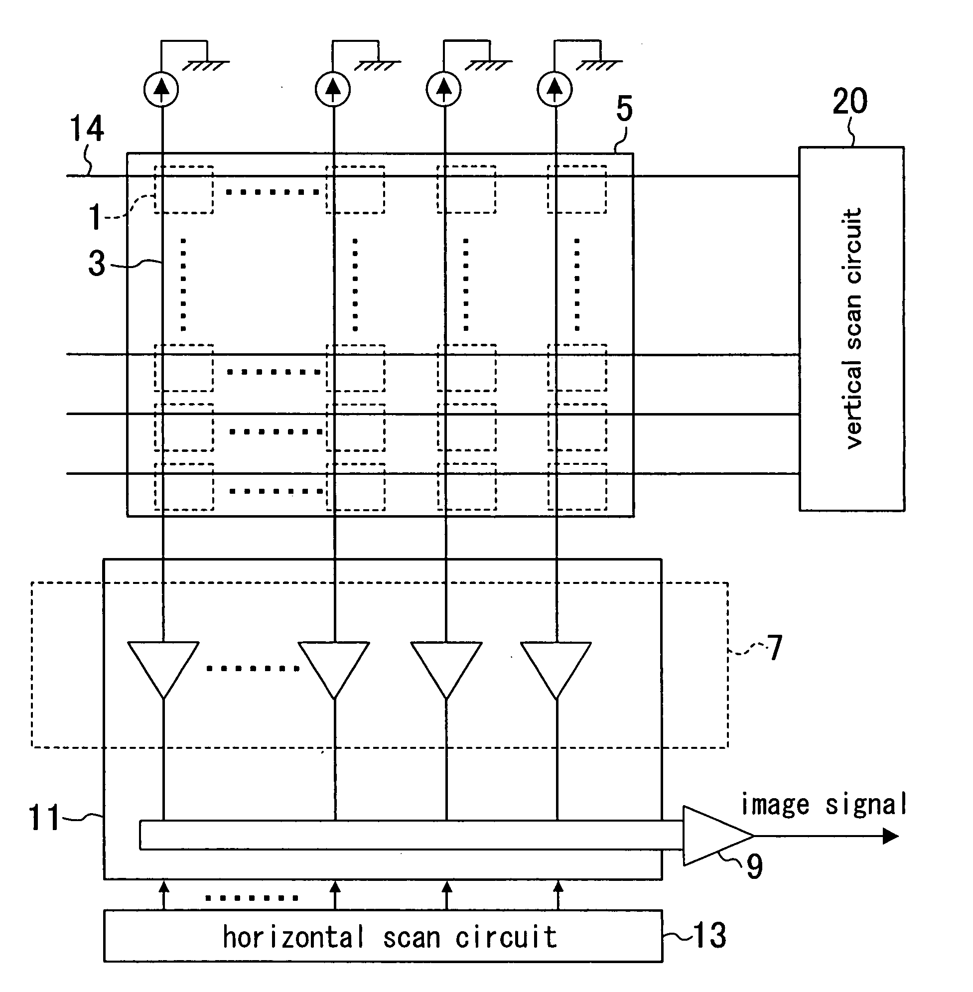
[0062]As shown in FIG. 3D, in the solid-state image sensing device of the present variation, the column amplification section 7 includes current sources 29-1, 29-2, . . . , and 29-n, instead of resistances. The current sources 29-1, 29-2, . . . , and 29-n are formed of p-channel type transistors and respectively connected to the drains of the amplification transistors 27-1, 27-2, . . . , and 27-n. The impedance on the power supply side of the amplifier is greater than the impedance on the ground side. Moreover, it is designed such that the reactance component on the power supply side of the amplifier and the reactance component on the ground ...

embodiment 2

[0065]FIG. 5A and FIG. 5B are circuit diagrams illustrating a structure of an amplification section of a solid-state image sensing device of Embodiment 2 of the present invention. The solid-state image sensing device of Embodiment 2 has the same structure as that of the solid-state image sensing device of Embodiment 1 excepting a structure between the column amplification section 7 and the power supply voltage feed section and a structure between the column amplification section 7 and the ground. Therefore, descriptions are given below only to the characteristic structures.

[0066]As shown in FIG. 5A and FIG. 5B, the column amplification section 7 of the solid-state image sensing device of Embodiment 2 is characterized in that the first resistive element is not provided on the power supply side of the amplifier 8, that is, between the amplifier 8 and the power supply voltage feed section AVDD or the power supply pad 21. The amplifier 8 is connected to the power supply voltage feed sec...

embodiment 3

[0073]FIG. 6A and FIG. 6B are circuit diagrams illustrating a structure of an amplification section of a solid-state image sensing device of Embodiment 3 of the present invention. The solid-state image sensing device of Embodiment 2 has the same structure as that of the solid-state image sensing device of Embodiment 1 excepting a structure between the column amplification section 7 and the power supply voltage feed section and a structure between the column amplification section 7 and the ground. Therefore, descriptions are given below only to the characteristic structures.

[0074]As shown in FIG. 6A and FIG. 6B, the column amplification section 7 of the solid-state image sensing device of Embodiment 3 is characterized in that a second resistive element is not provided on the power supply side of the amplifier 8, that is, between the amplifier 8 and the ground or the ground pad 23. The amplifier 8 is connected to the ground or the ground pad 23 by a general line which is the same as l...


PUM


Abstract

A solid-state image sensing device includes: a pixel array in which pixels performing photoelectric conversion are arranged in rows and columns; and a column amplification section in which an image signal output from each pixel is amplified. The column amplification section includes amplifiers each of which is provided for each column, and the column amplification section is connected to a power supply voltage feed section and the ground. An impedance on the power supply side of the amplifier is greater than an impedance on the ground side.

Description

BACKGROUND OF THE INVENTION[0001]1. Field of the Invention[0002]The present invention relates to a solid-state image sensing device and an image sensing device including the solid-state image sensing device.[0003]2. Description of the Prior Art[0004]In recent years, as an alternative image sensor of a CCD (Charge Coupled Device) type image sensor, a MOS type image sensor has been a subject of interest. This is because the MOS type image sensor has many advantages such as that steady supply of MOS type image transistor is possible because the MOS type image sensor can be fabricated by the same CMOS process as that used for CPU (Central Processing Unit) and memories, and thus existing equipment can be utilized; a drive circuit and a signal processing circuit can be more simply structured compared to the CCD type image sensor; and power consumption can be reduced.[0005]A general MOS type image sensor includes: a pixel array having pixels arranged in rows and columns and vertical signal...

Claims


Application Information

Patent Timeline
Patent Type & Authority Applications(United States)
IPC IPC(8): H04N5/335H01L27/146H04N5/357H04N5/369H04N5/374H04N5/3745H04N5/376
CPCH03F3/082H03F2200/498H04N5/378H04N5/335H03F2200/75H04N25/00H04N25/75H04N25/62H04N25/76
Inventor YOSHIDA, HIROSHIMATSUNAGA, YOSHIYUKIMUROSHIMA, TAKAHIRO
Owner PANASONIC SEMICON SOLUTIONS CO LTD
Why Eureka
Try Eureka