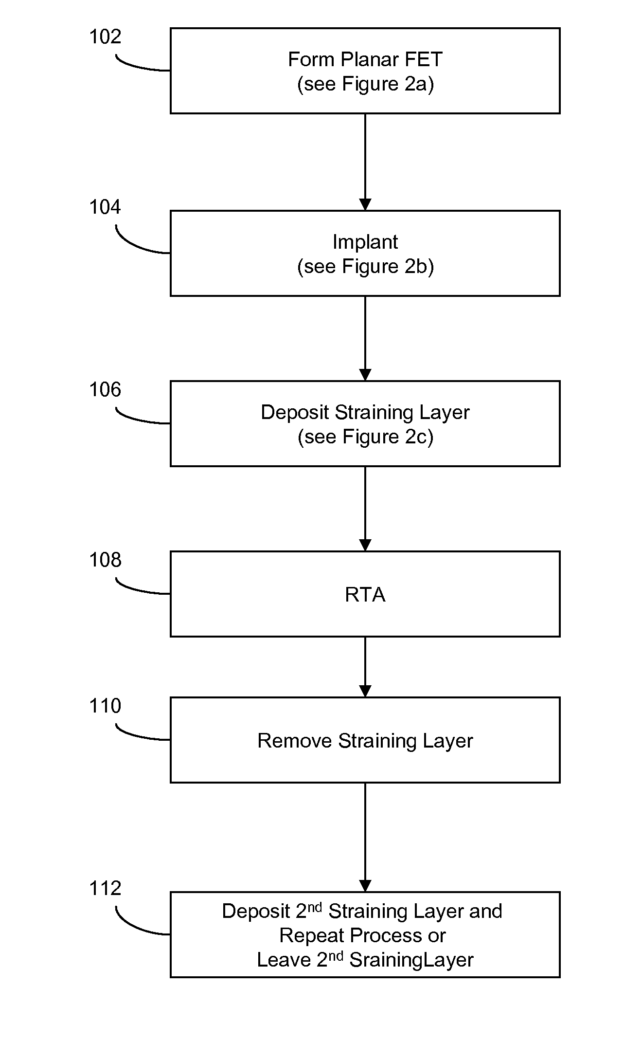
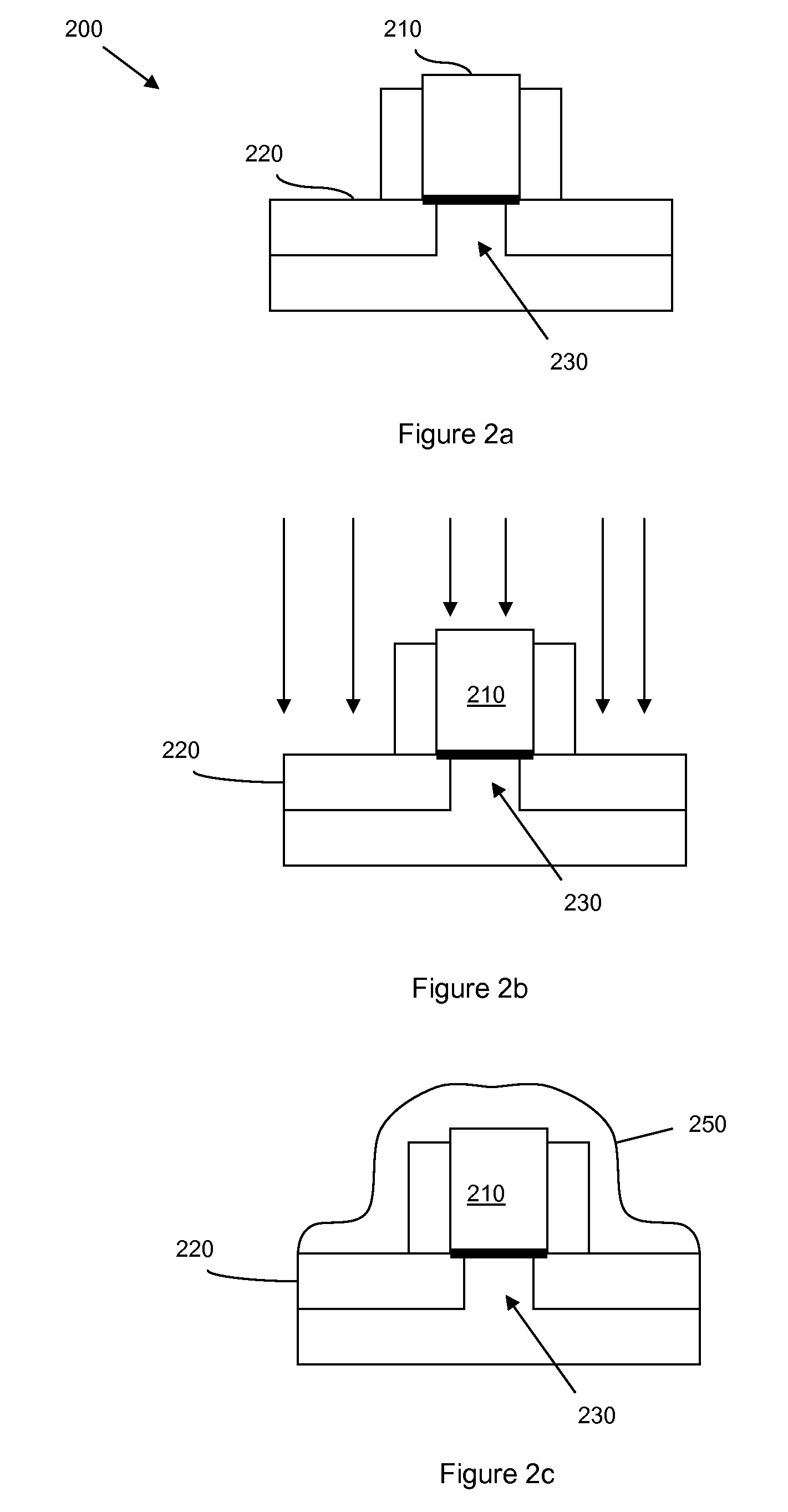
[0009] In view of the foregoing, disclosed herein are embodiments of a stress memorization technique suitable for use in the formation of one or more non-planar field effect transistors (FETs), such as fin-type field effect transistors (finFETs) and trigate FETs. The technique induces a selected strain in the
polysilicon gate electrode of a non-planar FET in order to impart a similar strain on the FET channel region and, thereby, optimize FET performance, while simultaneously protecting the source / drain regions of the semiconductor fin. Specifically, a protective cap layer is formed on the top surface of the source / drain regions of the fin in order to protect those regions during a subsequent amorphization
ion implantation process. The fin is further protected, during this implantation process, because the
ion beam is directed towards the gate in a plane that is parallel to the fin and tilted from the
vertical axis. Thus, amorphization of and damage to the fin are limited. Following the implantation process (which can occur either before or after the formation of a straining layer), a recrystallization anneal is performed so that the strain of the straining layer is ‘memorized’ in the polysilicon gate.
[0012] As with traditional stress memorization techniques, ions are implanted in order to amorphize the gate. However, the embodiments of the method that are disclosed herein provide a
novel technique for implanting the ions in order to further prevent damage to the fin and to limit amorphization of the source / drain regions of the fin. Specifically, the amophization
ion implantation process is accomplished by directing the ions towards the gate in a plane that is parallel to the plane containing the fin and by directing the ions at a non-perpendicular angle to the substrate (i.e., by tilting the
ion beam from the
vertical axis). The protective layer on the top surface of the fin prevents the ions from being implanted through the top surface of the source / drain regions. Additionally, by directing the
ion beam in the same plane as the fin and by tilting the ion beam from the vertical axis, the ions are directed into the opposing sidewalls of the gate and not into the opposing sidewalls of the fin. Thus, damage to the fin as well as complete amorphization of the source / drain regions of the fin is avoided.
[0013] An appropriate straining layer is then formed over the gate. Following both the
ion implantation process and the formation of the straining layer, a thermal anneal process can be performed in order to re-crystallize the gate as well as those portions of the semiconductor fin which may have been amorphized during the
ion implantation process. As mentioned above, this recrystallization process causes the strain of the straining layer to be ‘memorized’ in the polysilicon gate above the channel region and, thus, imparts a similar strain in the channel region of the fine. Following the recrystallization process, the straining layer may be removed. Optionally, after removing the first straining layer, a second straining layer can be formed over the FET structure and, particularly, over the gate to further enhance the strain in the channel region of the FET.
[0018] The protective
layers on the top surfaces of the fins prevent the ions from being implanted through the top surfaces of the source / drain regions. Additionally, by directing the ion beam in the same plane as the fins and by tilting the ion beam, the ions are directed into the opposing sidewalls of the gates and not into the opposing sidewalls of the fins. Thus, damage to the fins as well as complete amorphization of the source / drain regions of the fins is avoided.
[0020] After the first gate is amorphized, then the second semiconductor fin
and gate are unmasked and the first semiconductor fin
and gate are masked. The implantation process is then repeated. That is, ions are implanted into the second gate. Specifically, the ions are directed in an ion beam towards the second gate in a second plane that is parallel to the second semiconductor fin. The ions are also directed at a second non-perpendicular angle (e.g., between approximately 50 and 80 degrees) to the substrate. The angle is predetermined so that the implantation process is not blocked by any of the other features on the substrate (e.g., masks, other devices, etc.). The protective layer on the top surface of the second fin prevents the ions from being implanted through the top surfaces of the source / drain regions. Furthermore, by directing the ions in the same plane as the second fin and by tilting the ion beam, the ions are specifically directed towards the sidewalls of the second gate and not towards the sidewalls of the second semiconductor fin. Thus, damage to the fins as well as complete amorphization of the source / drain regions of the fins is avoided.
[0023] After the recrystallization process, the straining layer may be removed and another straining layer may be formed over the FET structures in order to further enhance the strain in the channel regions of each of the FETs.

