Light emitting apparatus

Inactive Publication Date: 2007-11-01
DELTA ELECTRONICS INC
View PDF11 Cites 98 Cited by
  • Summary
  • Abstract
  • Description
  • Claims
  • Application Information

AI Technical Summary

Benefits of technology

[0009]In view of the foregoing, the invention is to provide a light emitting apparatus, which can be manufactured simply and has high light emitting efficiency, high heat dissipating effect and reduced cost.
[0010]To achieve the above, the invention discloses a light emitting apparatus including a substrate, at least one light emitting device and a protective layer. The substrate is formed with a structure for increasing light emitting efficiency. The light emitting device is disposed at a predetermined position on the substrate, and the protective layer covers the light emitting device.
[0011]As mentioned hereinabove, the light emitting device is disposed at the predetermined position of the substrate in the light emitting apparatus according to the present invention. The light emitting efficiency is enhanced beca

Problems solved by technology

When the conventional LED light emitting apparatus 1 emits lights, parts of the lights leaks from the lateral side of the light emitting device 12 and t

Method used


Image

  • Light emitting apparatus
  • Light emitting apparatus
  • Light emitting apparatus

Examples


Example

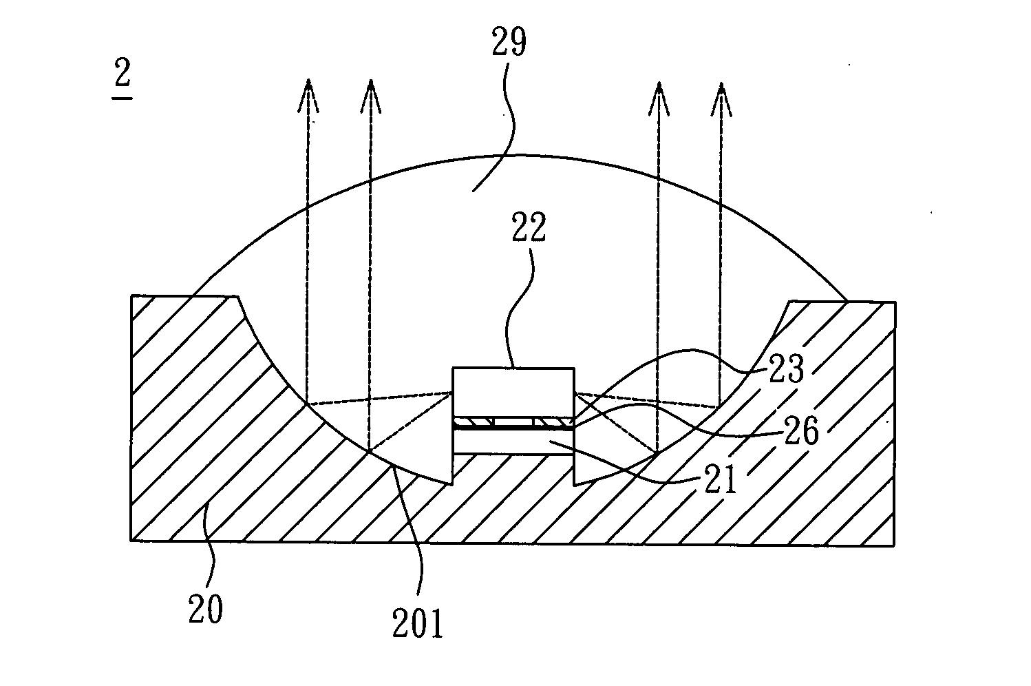
[0016]Referring to FIG. 2, a light emitting apparatus 2 according to a first embodiment of the invention includes a substrate 20, a first insulating layer 21, a connecting layer 26, a first metal layer 23, at least one light emitting device 22 and a protective layer 29.

[0017]In this embodiment, the material of the substrate 20 may be composed of copper, aluminum, magnesium, titanium or alloys thereof so as to provide a better thermal conductive effect. Alternatively, the material of the substrate 20 may be a ceramic material to provide a better thermal conductivity. The surface of the substrate 20 is formed with a structure 201 for increasing light emitting efficiency.

[0018]In this embodiment, the first insulating layer 21 is disposed at a predetermined position of the substrate 20 and may be formed by patterning the insulating layer 21 with a yellow photolithography process or a screen printing process, such that the structure 201 of the substrate 20 is partially exposed. The insul...

Example

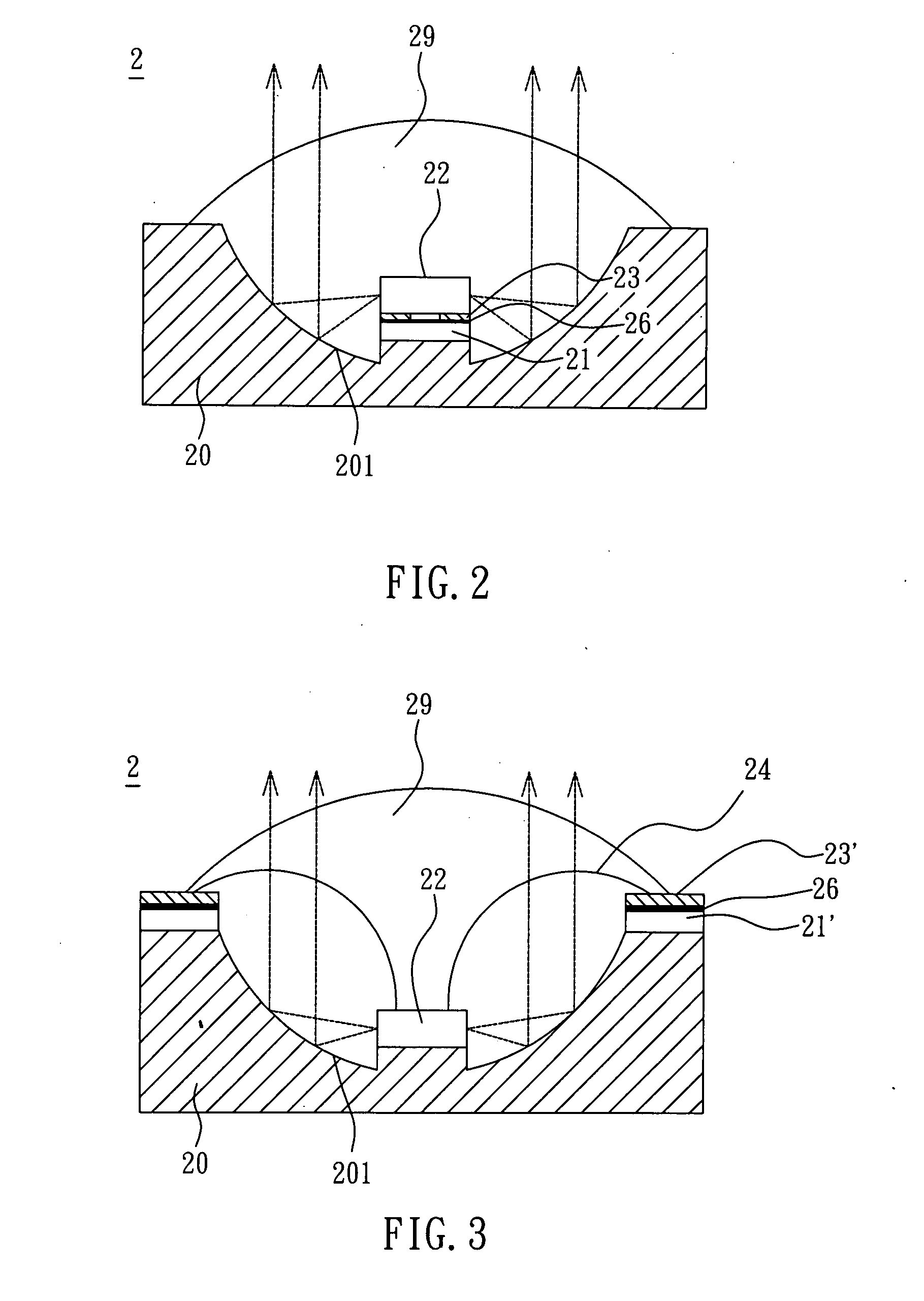
[0024]In addition, the invention provides the second embodiment, shown in FIG. 3, in which the light emitting apparatus 2 includes a second insulating layer 21′ disposed out of the structure 201 of the substrate 20. Similarly, the insulating layer 21′ may be formed by patterning the insulating layer 21 by, for example, yellow photolithography or screen printing. The material of the insulating layer 21 may be aluminum oxide, magnesium oxide, titanium oxide, aluminum nitride, magnesium nitride, titanium nitride, aluminum carbide, magnesium carbide, titanium carbide, or their combinations, and may be deposited by oxidizing, nitridizing or carbidizing the surface of the substrate or by way of evaporating, sputtering or chemical vapor deposition (CVD) on the substrate 20. That is, when the material of the substrate 20 is selected from at least one of aluminum, magnesium, titanium and alloys thereof, the insulating layer 21′ may be formed by oxidizing, nitridizing or carbidizing the surfa...


PUM


Abstract

A light emitting apparatus includes a substrate, at least one light emitting device and a protective layer. The substrate has a surface formed with a structure for increasing light emitting efficiency. The light emitting device is disposed on a predetermined position of the substrate. The light emitting device emits lights and the lights are reflected and concentrated to project out by the structure of the substrate. Thus, the light emitting efficiency is improved.

Description

CROSS REFERENCE TO RELATED APPLICATIONS [0001]This Non-provisional application claims priority under 35 U.S.C. §119(a) on Patent Application No(s). 09 / 5115257 filed in Taiwan, Republic of China on Apr. 28, 2006, the entire contents of which are hereby incorporated by reference.BACKGROUND OF THE INVENTION[0002]1. Field of Invention[0003]The invention relates to a light emitting apparatus, and in particular to a light emitting apparatus having good heat dissipating efficiency.[0004]2. Related Art[0005]With the development of the opto-electronic industry, light emitting devices, such as LEDs (Light Emitting Diodes), have been widely and variously applied to display functions of electronic products.[0006]Referring to FIG. 1, a conventional LED light emitting apparatus 1 includes a substrate 10, an insulating layer 11, a plurality of LED light emitting devices 12, a first metal layer 13 and a package layer 14. The insulating layer 11 is disposed on the substrate 10. The light emitting de...

Claims


Application Information

Patent Timeline
IPC IPC(8): H01L33/00H01L33/56F21V29/505H01L33/60H01L33/62H01L33/64
CPCH01L33/60H01L2224/48091H01L2924/01012H01L2924/01029H01L2924/01078H01L2924/04941H01L2924/01079H01L2924/00014H01L2924/12044H01L2924/00
Inventor CHANG, SEANCHEN, YU-CHUAN
Owner DELTA ELECTRONICS INC
Why Eureka
Try Eureka