Electric Circuit Device, Electric Circuit Module, and Power Converter

a technology of electric circuit module and circuit device, which is applied in the directions of semiconductor/solid-state device details, fixed capacitor details, transportation and packaging, etc., can solve the problems of increasing the heat capacity of the semiconductor chip, generating a large amount of heat, and increasing the heat generation of the semiconductor chip

Active Publication Date: 2007-11-01
HITACHI ASTEMO LTD
View PDF43 Cites 62 Cited by
  • Summary
  • Abstract
  • Description
  • Claims
  • Application Information

AI Technical Summary

Problems solved by technology

However, semiconductor chips generate a large amount of heat during an electrical conducting state, and as the chips are dimensionally reduced, they correspondingly increase in heat capacity and hence in the amount of heat generated.
The amount of heat generated by the semiconductor chips is also increased by the internal line inductance of the electric circuit device and by electrical loss due to the line inductance occurring at the input side of the electric circuit device during operation.
At present, therefore, the conventional techniques are not as effective as they can attain both of the above two factors.

Method used


Image

  • Electric Circuit Device, Electric Circuit Module, and Power Converter
  • Electric Circuit Device, Electric Circuit Module, and Power Converter
  • Electric Circuit Device, Electric Circuit Module, and Power Converter

Examples


first embodiment

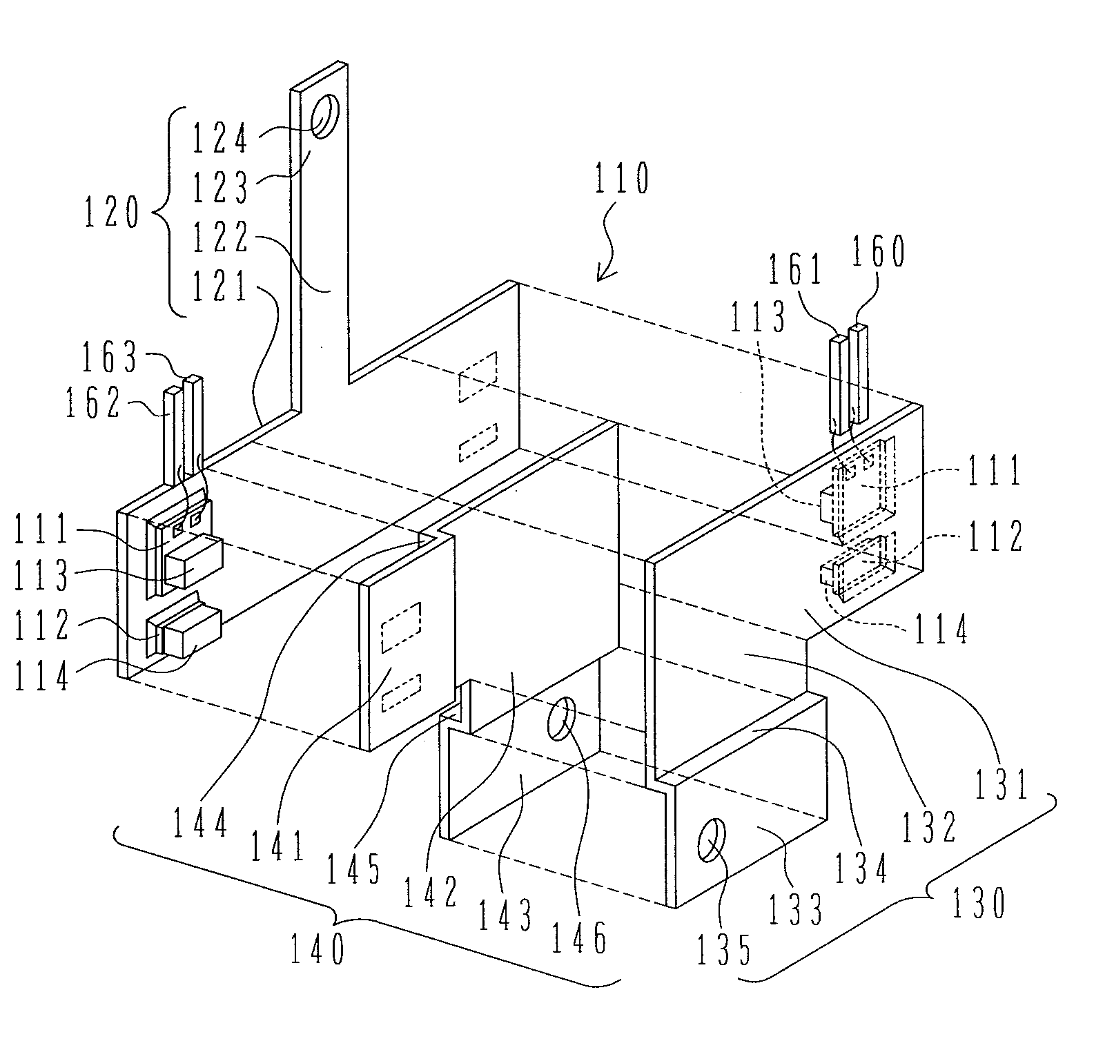
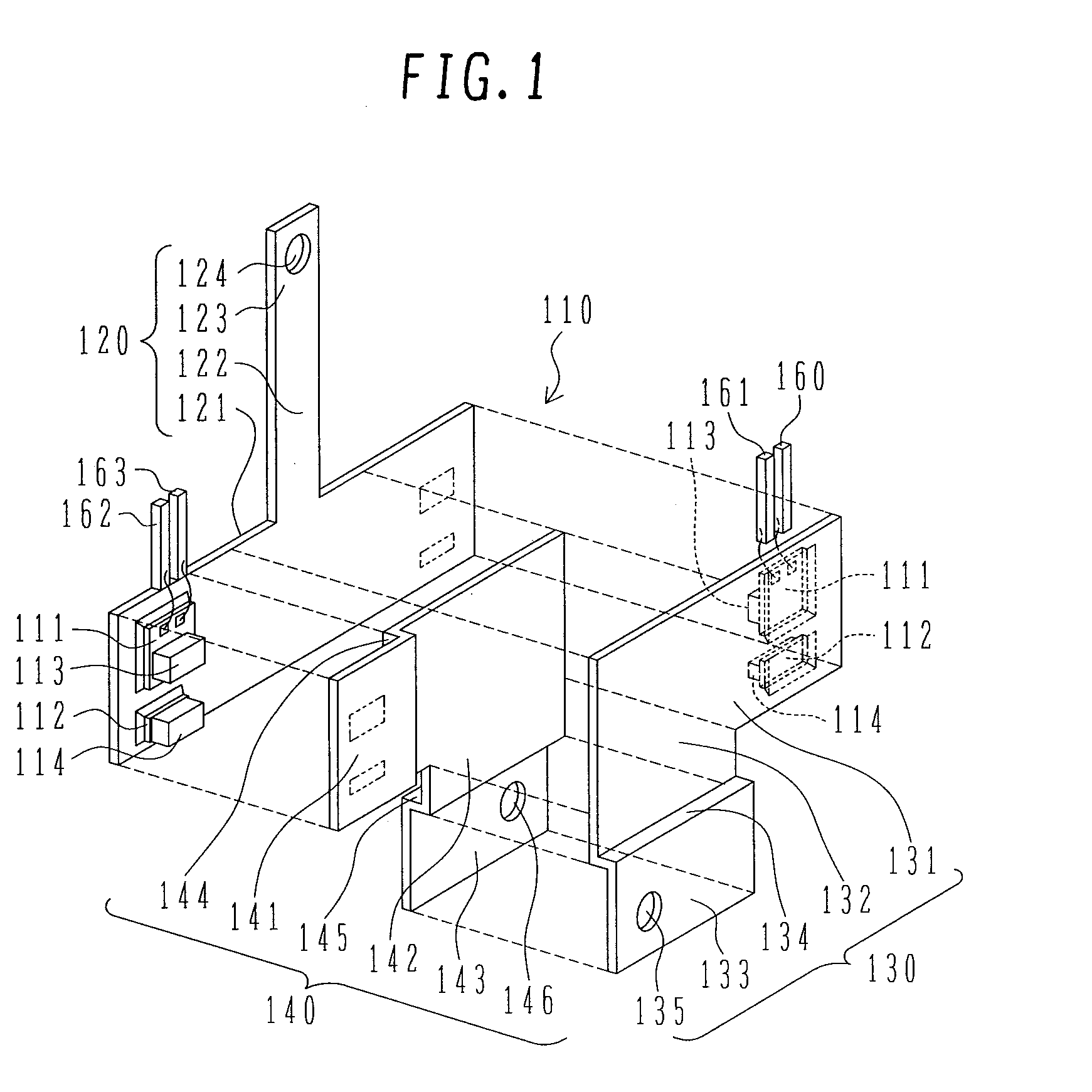
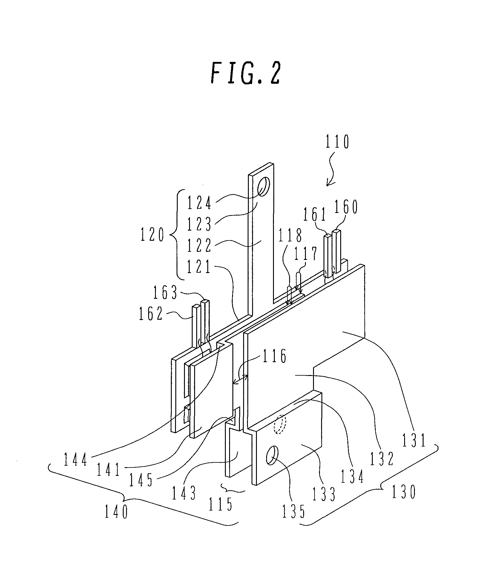
[0059]Hereunder, a first embodiment of the present invention will be described in accordance with FIGS. 1 to 20.

[0060]First, a configuration of a hybrid electric automobile 1 is described below using FIG. 20.

[0061]The hybrid electric automobile (hereinafter, referred to as HEV) 1 of the present embodiment is one electric vehicle and has two vehicular driving systems. One of them is an engine system that uses an internal-combustion engine 10 as a motive power source. The engine system is used as a driving source of the HEV. The other is a vehicular electric machine system that use motor generators 30, 40 as motive power sources. The vehicular electric machine system is primarily used as another driving source of the HEV and as an electric power generator for the HEV.

[0062]At a front section of a vehicle body (not shown), front wheel axles 3 are axially supported so as to be rotatable. One pair of front wheels 2 are disposed at both ends of each front wheel axle 3. At a rear section o...

second embodiment

[0180]A second embodiment of the present invention will be described per FIG. 21.

[0181]The present embodiment, an improvement of the first embodiment, is an example of transposing the configurations of the P-electrode 130 and N-electrode 140 of the first embodiment. The present (second) embodiment differs from the first embodiment in three respects. One is that a configuration of a first bend 136 is added to the P-electrode 130 (however, the first bend 136 differs from the first bend 144 of the first embodiment in terms of position and is opposite in extending direction of a conductor). One is that the configuration of the lead wire 132 is replaced with a configuration of a lead wire 142 in the first embodiment (however, the lead wire 132 is opposite to the lead wire 142 of the first embodiment in terms of extending direction of a conductor). One is that since the first bend is removed from the N-electrode 140, the configuration of the lead wire 142 is replaced with a configuration ...

third embodiment

[0183]A third embodiment of the present invention will be described per FIG. 22.

[0184]The present embodiment, an application of the first embodiment, is an example of connecting arms' IGBTs 111 and diodes 112 in two lines in parallel. In the present (third) embodiment, the same pair of chips as that of HI and HD chips juxtaposed in a short-side direction are juxtaposed in a long-side direction, and the same pair of chips as that of LI and LD chips juxtaposed in a short-side direction are juxtaposed in a long-side direction. Along with these, the number of G-wires 160, 162 and S-wires 161, 163 is also correspondingly increased. In the present embodiment, various electrodes have areas larger than those of the electrodes in the first embodiment. Other elements are the same as those of the first embodiment in terms of configuration, so the same reference number or symbol is assigned to the same element, description of which is omitted.

[0185]In the present embodiment described above, as ...


PUM


Abstract

The present invention provides an electric circuit device in which it is possible to achieve simultaneously the improvement of cooling performance and reduction in operating loss due to line inductance.
The above object can be attained by constructing multiple plate-like conductors so that each of these conductors electrically connected to multiple semiconductor chips is also thermally connected to both chip surfaces of each such semiconductor chip to release heat from the chip surfaces of each semiconductor chip, and so that among the above conductors, a DC positive-polarity plate-like conductor and a DC negative-polarity plate-like conductor are opposed to each other at the respective conductor surfaces.

Description

BACKGROUND OF THE INVENTION[0001]1. Field of the Invention[0002]The present invention relates to an electric circuit device adapted to configure an electric circuit that uses semiconductors, an electric circuit module with the device mounted therein, and an electric power converter having the module.[0003]2. Description of the Related Art[0004]Known techniques related to an electric circuit device adapted to configure an electric circuit that uses semiconductors, an electric circuit module having the device mounted therein, and an electric power converter having the module, are described in JP-A-2004-208411, JP-A-2004-193476, and JP-A-10-248266, for example. JP-A-2004-208411 discloses the technique for sandwiching high-side semiconductor chips (IGBT chip and diode chip) and low-side semiconductor chips (IGBT chip and diode chip) by use of a common middle-side plate and high-side plate and a common middle-side plate and low-side plate, respectively, and cooling each of the semiconduc...

Claims


Application Information

Patent Timeline
Patent Type & Authority Applications(United States)
IPC IPC(8): H01L29/74
CPCH02M7/003H01L2224/45124H01L2924/1305H05K7/02H01L2924/3025H01L2924/30107H01L2224/73265H01L2224/73215H01L2224/48247H01L2224/32245H01L2924/13091H01L2924/13055H01L2224/48091H01L2924/00014H01L2924/00H01L2924/00012H01L2924/181H01L24/73H01L2924/14H01G2/08H01G4/224Y02T10/70
Inventor TOKUYAMA, TAKESHINAKATSU, KINYAKAWABATA, ATUSHI
Owner HITACHI ASTEMO LTD
Why Eureka
Try Eureka