Spin accumulation device and magnetic sensor applied with spin current confined layer

a magnetic sensor and spin current technology, applied in the field of spin accumulation devices, can solve the problems of insufficient output amplitude, inability to achieve an increased output, and the tunneling junction for achieving an increased output does not provide a function as an external magnetic field sensor, etc., to achieve high sensitivity, reduce electric noise, and high resolution

Inactive Publication Date: 2007-11-01
HITACHI LTD
View PDF9 Cites 32 Cited by
  • Summary
  • Abstract
  • Description
  • Claims
  • Application Information

AI Technical Summary

Benefits of technology

[0015]Based on the current confined layer in the case of the CPP-GMR, since an electrical current is confined and caused to flow, electrical current density is high in a pinhole portion. Thus, it is problematic in that the pinhole portion is deteriorated due to Joule's heat or the like. However, based on the spin current confined layer according to the present invention, since no electrical current flows, such problem does not occur. Further, instead of an electrical current, since the spin current flows through the spin current

Problems solved by technology

However, such output amplitude is insufficient for a terabit-level magnetic recording and reproducing head, and therefore a spin accumulation device having an even higher output is needed.
Further, based on the spin accumulation device using the tunneling junction, since th

Method used


Image

  • Spin accumulation device and magnetic sensor applied with spin current confined layer
  • Spin accumulation device and magnetic sensor applied with spin current confined layer
  • Spin accumulation device and magnetic sensor applied with spin current confined layer

Examples


example 1

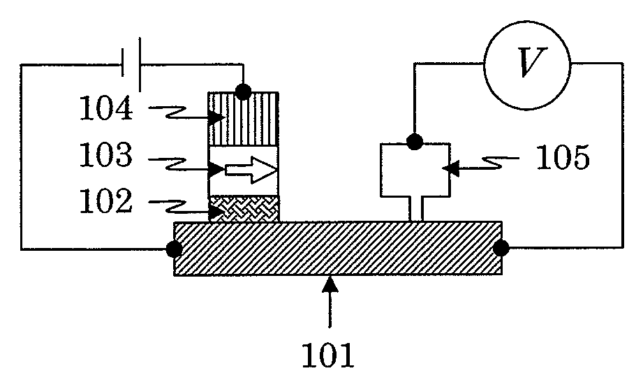
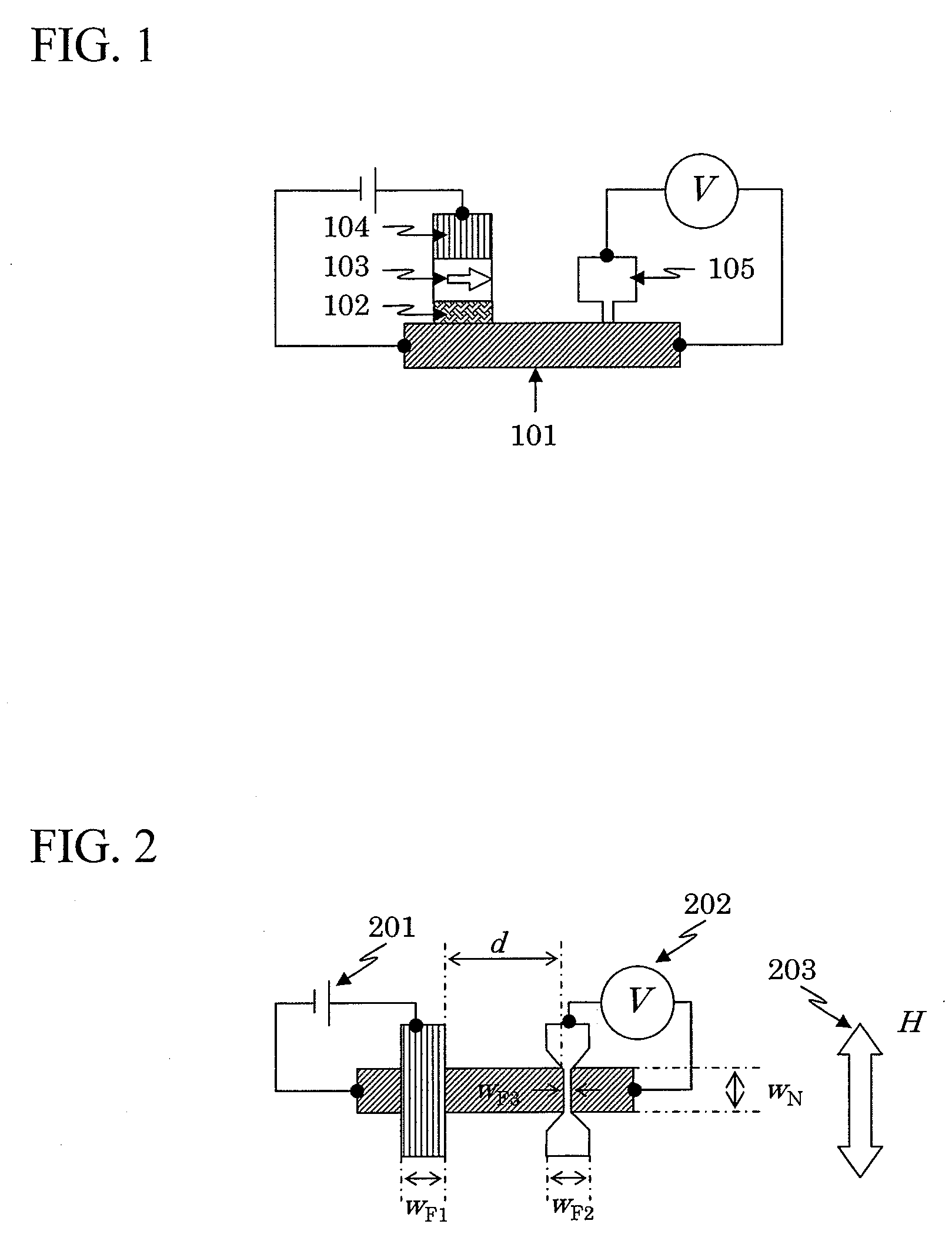
[0028]FIG. 1 shows a sectional side view of a spin accumulation device according to a first example of the present invention, and FIG. 2 shows a plan view of the device. The spin accumulation device is structured so that a nonmagnetic conductive material 101 and a first magnetic conductive material 103 are in contact with an insulating barrier layer 102 formed on the nonmagnetic conductive material 101 and so that a second magnetic conductive material 105 is in contact with the nonmagnetic conductive material 101 at another location. Magnetization of the first magnetic conductive material 103, which functions as a spin injection source, is magnetically fixed by an anti-ferromagnetic material 104. A voltage induced by the spin accumulation effect in the nonmagnetic conductive material 101 is detected between the second magnetic conductive material 105 and the above nonmagnetic conductive material 101. The voltage-detection second magnetic conductive material 105 was formed so that it...

example 2

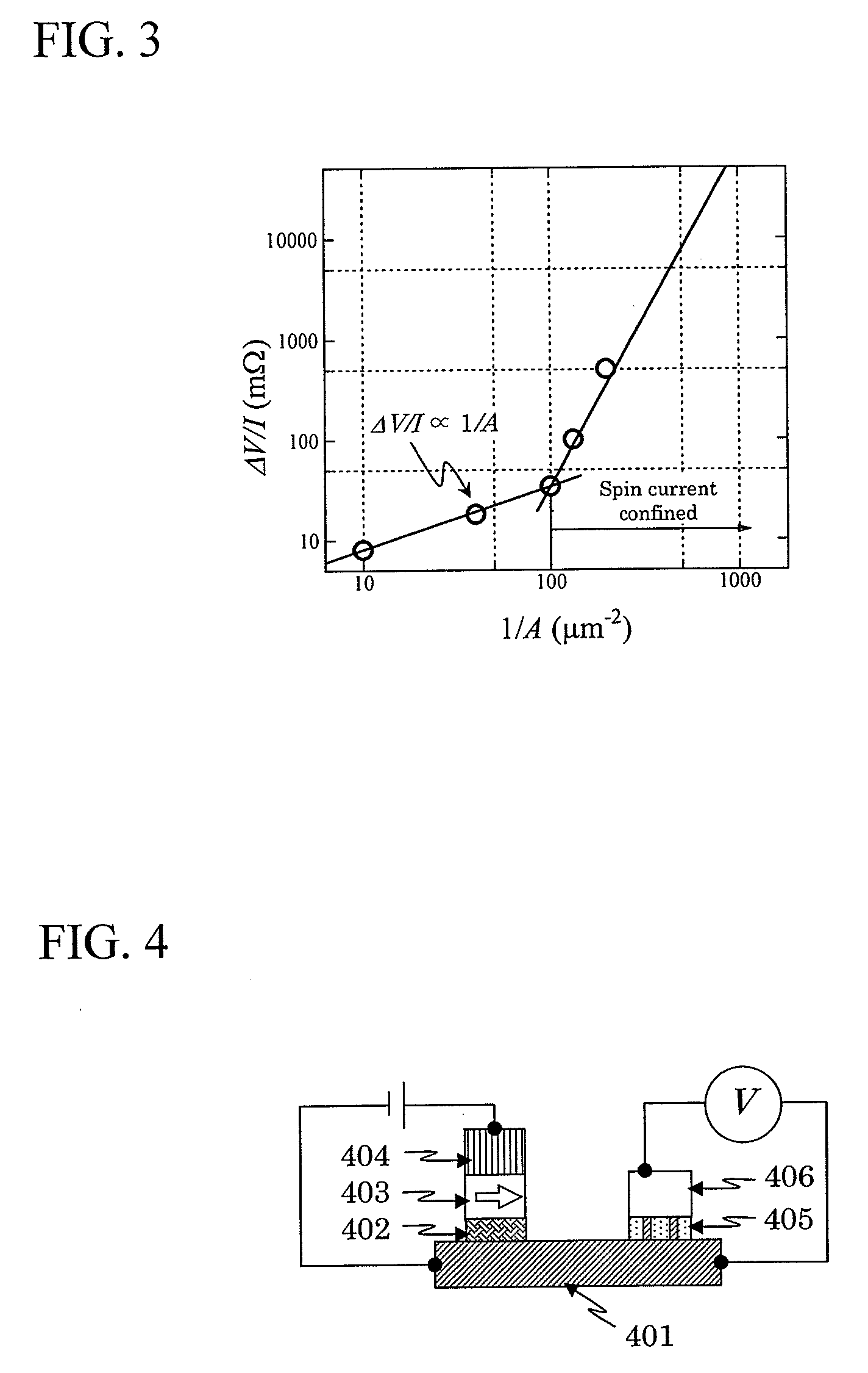
[0039]FIG. 4 shows a sectional side view of a spin accumulation device according to a second example of the present invention, and FIG. 5 shows a plan view of the device. This spin accumulation device is provided with a spin current confined layer 405 between a voltage-detection magnetic conductive material 406 and a nonmagnetic conductive material 401 (see FIG. 6). The nonmagnetic conductive material 401, an insulating barrier layer 402, a magnetic conductive material 403, and an anti-ferromagnetic material 404 used in the present example were the same as those used in Example 1.

[0040]As shown in FIG. 5, the junction area of the spin current confined layer 405 and the nonmagnetic conductive material 401 is defined by A2′=wN×wF2. Note that the junction area A2′ was obtained by measuring the wire width wN of the nonmagnetic wire and the wire width wF2 of the magnetic wire with an atomic force microscopy. Reference numerals 501 and 502 denote a DC current source and a voltage detector...

example 3

[0046]FIG. 8 shows a sectional side view of a spin accumulation device according to a third example of the present invention. Based on the present spin accumulation device, a magnetic conductive material 802 that injects a current 806 and a nonmagnetic conductive material 801 are electrically in direct contact with each other. The nonmagnetic conductive material 801, magnetic conductive materials 802 and 805, and an anti-ferromagnetic material 803 used in the present example were the same as those used in Example 1, and a spin current confined layer 804 used in the present example was the same as that used in Example 2. Since the nonmagnetic conductive material 801 and the magnetic conductive material 802 are electrically in direct contact with each other, a low-noise spin accumulation device can be obtained. Additionally, since the spin current confined layer 804 is used, higher output can be achieved as in Example 2.


PUM


Abstract

A spin accumulation device with high output, high resolution, and low noise. A spin current confined layer is located between a voltage-detection magnetic conductive material and a nonmagnetic conductive material. A spin current alone flows through the spin current confined layer. Due to the confinement of the spin current, since it is possible to prevent the spin current from flowing through excess portions other than the scatterer that exhibits resistance change, the detection efficiency of the spin accumulation device is dramatically increased.

Description

CLAIM OF PRIORITY[0001]The present application claims priority from Japanese application JP 2006-121663 filed on Apr. 26, 2006, the content of which is hereby incorporated by reference into this application.BACKGROUND OF THE INVENTION[0002]1. Field of the Invention[0003]The present invention relates to a spin accumulation device and a method for manufacturing the same.[0004]2. Background Art[0005]In the market of magnetic recording and reproducing apparatus, improvement in recording density is demanded by an annual rate of more than 40%, and it is estimated that Tbit / in2 will be reached by the year of 2010 or so in accordance with the current rate of growth. Higher output or higher resolution is demanded for a magnetic recording and reproducing head mounted on a terabit-level magnetic recording and reproducing apparatus. Regarding a current magnetic recording and reproducing apparatus, as an element technology, a CPP-GMR (Current Perpendicular to Plane Giant Magneto Resistance) head...

Claims


Application Information

Patent Timeline
IPC IPC(8): G11B5/33
CPCB82Y25/00H01F41/34G01R33/093G01R33/09H10N50/00
Inventor YAMADA, MASAKITAKAHASHI, HIROMASA
Owner HITACHI LTD
Why Eureka
Try Eureka