Apparatuses for dissipating heat from semiconductor devices

a technology for semiconductor devices and apparatuses, applied in the direction of electrical apparatus construction details, lighting and heating apparatuses, indirect heat exchangers, etc., can solve the problems of limited surface area available for cooling vapor, difficult machine, and high manufacturing cost of materials with better properties than aluminum, so as to improve the two-phase cooling efficiency and increase the surface area of the vapor chamber

Active Publication Date: 2007-11-08
GLOBALFOUNDRIES US INC
View PDF23 Cites 74 Cited by
  • Summary
  • Abstract
  • Description
  • Claims
  • Application Information

AI Technical Summary

Benefits of technology

[0011] Aspects of the invention relate to a fin-shaped vapor chamber for efficient two-phase heat transfer. More specifically, aspects of the invention disclose a wick-assisted three-dimensional (3D) shaped (e.g., fin-shaped) vapor chamber structure that can be combined with other cooling mechanisms to provide efficient two-phase heat transfer for semiconductor devices. Based on the chip orientation and package configuration, a plurality of hollow fin designs are proposed to increase the surface area of vapor chamber and improve the two-phase cooling efficiency relative to conventional h

Problems solved by technology

However, most materials that offer better properties than aluminum often are expensive to manufacture.
For example, copper (390 W/m-K) offers higher thermal conductivity than aluminum (230 W/m-K), but it weighs 3 times heavier and is more diffic

Method used


Image

  • Apparatuses for dissipating heat from semiconductor devices
  • Apparatuses for dissipating heat from semiconductor devices
  • Apparatuses for dissipating heat from semiconductor devices

Examples


Embodiment Construction

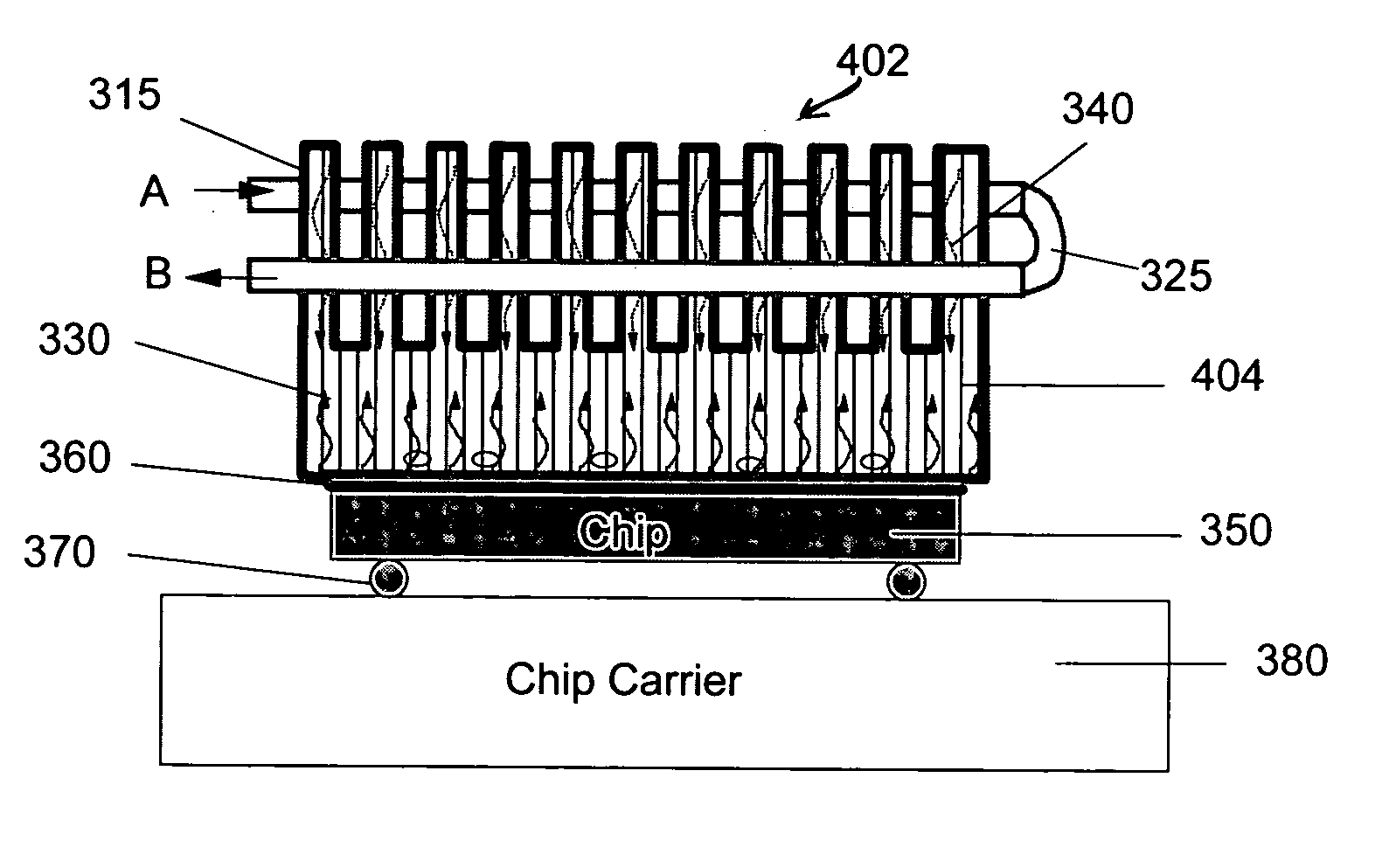
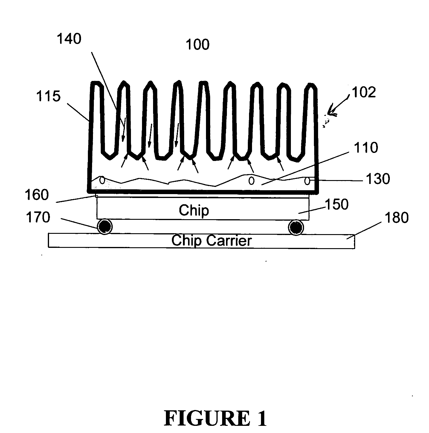
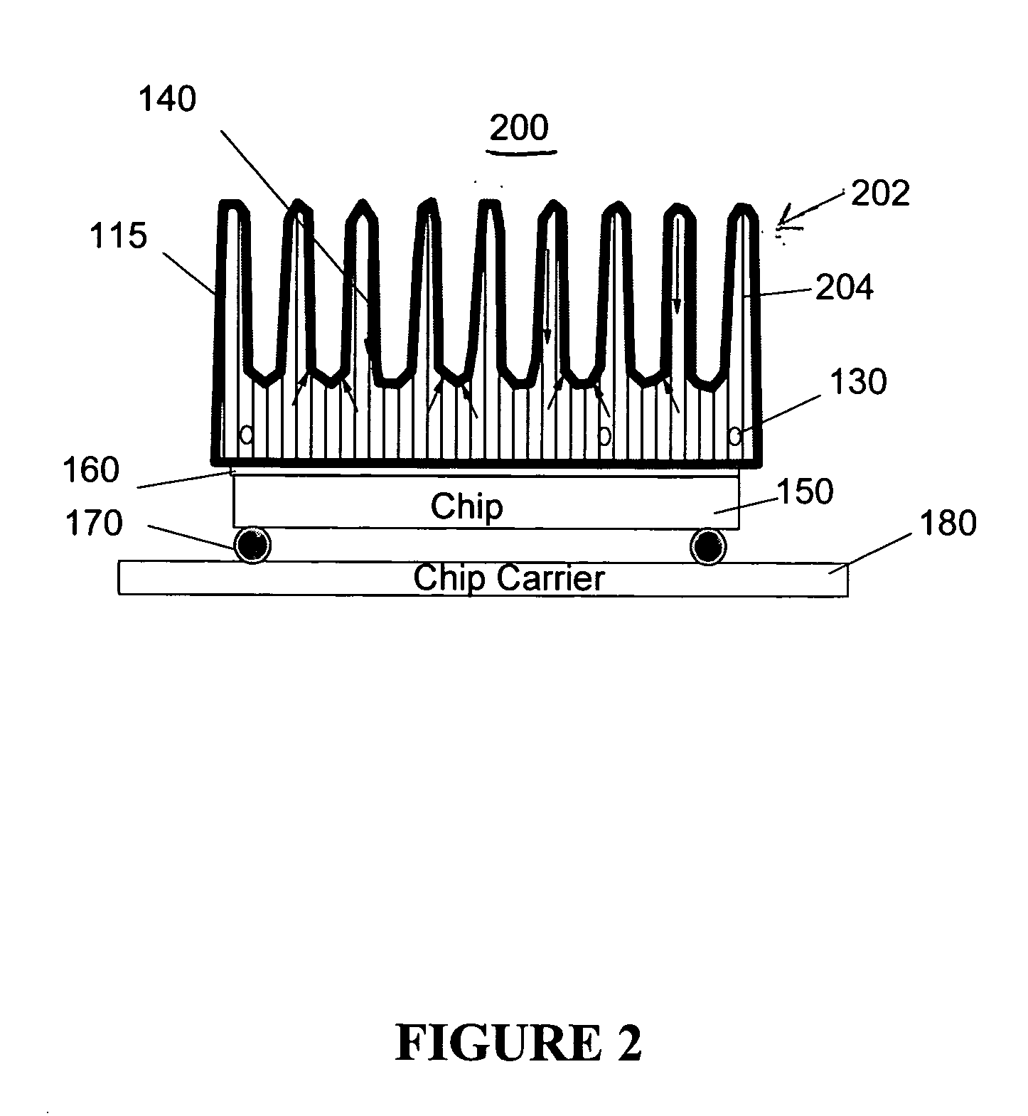
[0026] Referring to FIG. 1, there is shown a perspective view of a heat dissipation module 100. The module 100 includes an air-cooled fin-shaped hollow heat sink 102 that is partially filled with working fluid in accordance with an exemplary embodiment of the invention. The heat sink 102 has a base section in close proximity to a chip, a plurality of three-dimensional (3D) shaped members 115. In one exemplary embodiment, the 3D shaped members 115 can be in the form of fin-shaped members. Other 3D shapes can be used. The heat sink 102 includes a large surface area but with an enclosed cavity inside. The heat sink 102 is also referred herein as a vapor chamber that can be manufactured by using, for example, molding, welding, or other low-cost means to form an extrusion-type heat sink container with a large surface area. However, instead of using a solid fin structure, the fins 115 are constructed with a hollow chamber connected to a base chamber so that vapor carrying latent heat can ...


PUM


Abstract

An apparatus for providing two-phase heat transfer for semiconductor devices includes a vapor chamber configured to carry a cooling liquid, the vapor chamber having base section, and a plurality of three-dimensional (3D) shaped members. The plurality of 3D-shaped members have interior and exterior sidewalls, the 3D-shaped members being connected to the base section so that vapor carrying latent heat can reach the respective interior sidewalls and get transferred to the respective exterior sidewalls configured to be in contact with an external coolant. The vapor chamber is configured to be in contact with a semiconductor device in order to remove heat therefrom.

Description

BACKGROUND OF THE INVENTION [0001] 1. Field of the Invention [0002] Aspects of the invention generally relate to heat transfer and, more specifically, to vapor chamber structures for efficient dissipation of heat from semiconductor devices. [0003] 2. Description of Related Art [0004] Removal of excessive heat from electronic packages using heat sinks is known in the semiconductor industry. To meet the increasing demand of heat flux density for high-power electronic products, various heat sink designs have been used. For example, tall, thin, flat fins can provide more cooling surface area for convective heat removal, and lower pressure drop for greater airflow. Further, the heat transfer coefficient (measured in watts per surface area per degree Celsius), and the temperature gradient, can be increased by crosscutting flat fins into multiple short sections if the direction of airflow is random. The leading and trailing edges of a fin can be augmented with a curvature on the surface to...

Claims


Application Information

Patent Timeline
IPC IPC(8): H05K7/20
CPCF28D15/0233F28D15/0275H01L2224/16225H01L23/427F28F2215/06F28D15/04
Inventor CHEN, HOWARDLIU, HSICHANGHSU, LOUISMOK, LAWRENCE
Owner GLOBALFOUNDRIES US INC
Why Eureka
Try Eureka