Method and apparatus for cooling semiconductor device hot blocks and large scale integrated circuit (IC) using integrated interposer for IC packages

a technology of integrated circuits and semiconductor devices, applied in electrical apparatus, semiconductor devices, semiconductor/solid-state device details, etc., can solve the problems of power consumption, on-chip power dissipation will continue to rise, and the operating voltage cannot be reduced

Active Publication Date: 2007-11-22
AVAGO TECH INT SALES PTE LTD
View PDF97 Cites 57 Cited by
  • Summary
  • Abstract
  • Description
  • Claims
  • Application Information

AI Technical Summary

Benefits of technology

[0017]Methods, systems, and apparatuses for improve

Problems solved by technology

Because of the increased difficulties in controlling noise margins as voltage decreases, operating voltages can no longer be reduced as quickly as in the past for 130 nm gate lengths and smaller.
Consequently, on-chip power dissipation will continue to rise.
With the increased use of 65 nm technology in foundry processes and the commercialization of 45 nm technology, power consumption is now a major technical problem facing the semiconductor industry.
Higher power density blocks create an uneven temperature distribution and lead to “hotspots,” also known as “hot blocks,” on the chip.
Also, if uniform carrier mobility is not achieved across the IC die due to on-chip temperature variations across the die, this may result in variations in signal speed and in complicating circuit timing control.
These methods are ofte

Method used


Image

  • Method and apparatus for cooling semiconductor device hot blocks and large scale integrated circuit (IC) using integrated interposer for IC packages
  • Method and apparatus for cooling semiconductor device hot blocks and large scale integrated circuit (IC) using integrated interposer for IC packages
  • Method and apparatus for cooling semiconductor device hot blocks and large scale integrated circuit (IC) using integrated interposer for IC packages

Examples


example embodiments

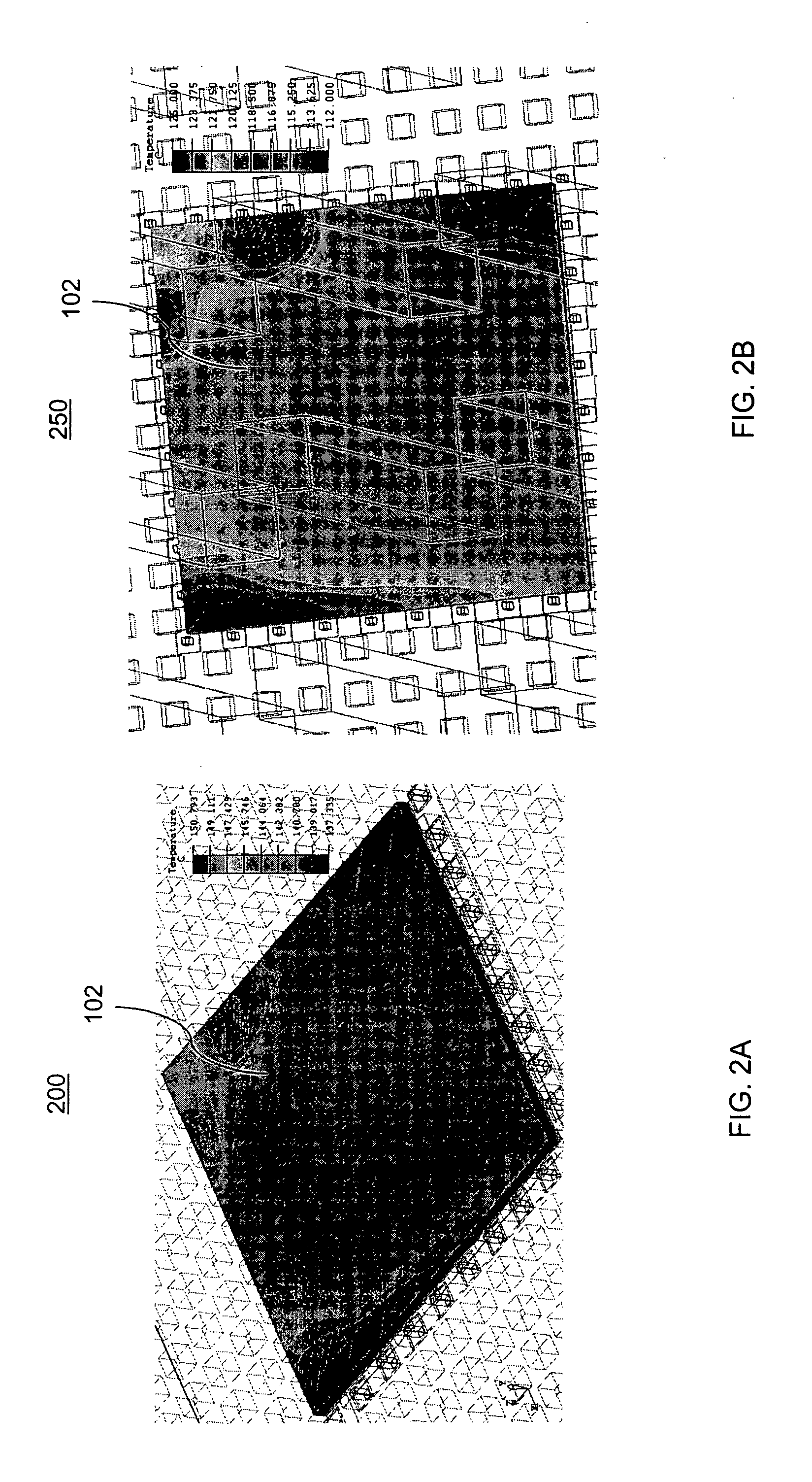
[0043]The present invention relates to the selective removal of heat from localized areas on an integrated circuit (IC) die. In an embodiment, a thermally conductive interposer structure is coupled to at least one contact pad on an IC die. The contact pad(s) are located at hotspots on the die. In further embodiments, the interposer is electrically and / or thermally conductive. In embodiments, the interposer is coupled to the die through thermal interconnect members (also referred to as thermal interconnects or nodules), which are thermally conductive balls, bumps, or blocks which are attached onto the interposer and / or the IC die during assembly. In a further embodiment, the nodules are thermally and / or electrically conductive. In an embodiment, the interposer is thermally and / or electrically coupled to the IC die.

[0044]In an embodiment, the interposer is coupled to an IC die at selected locations, such as blocks (e.g., areas on the surface of the die) with a high density of power di...

example ic package embodiments

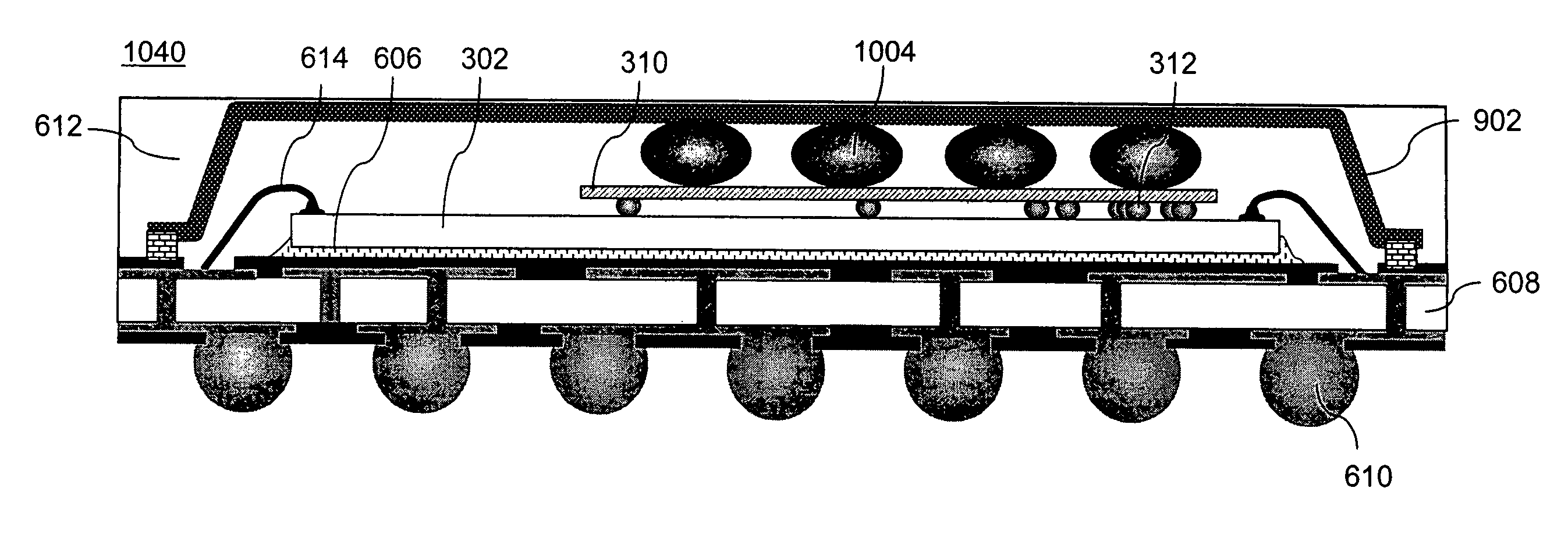
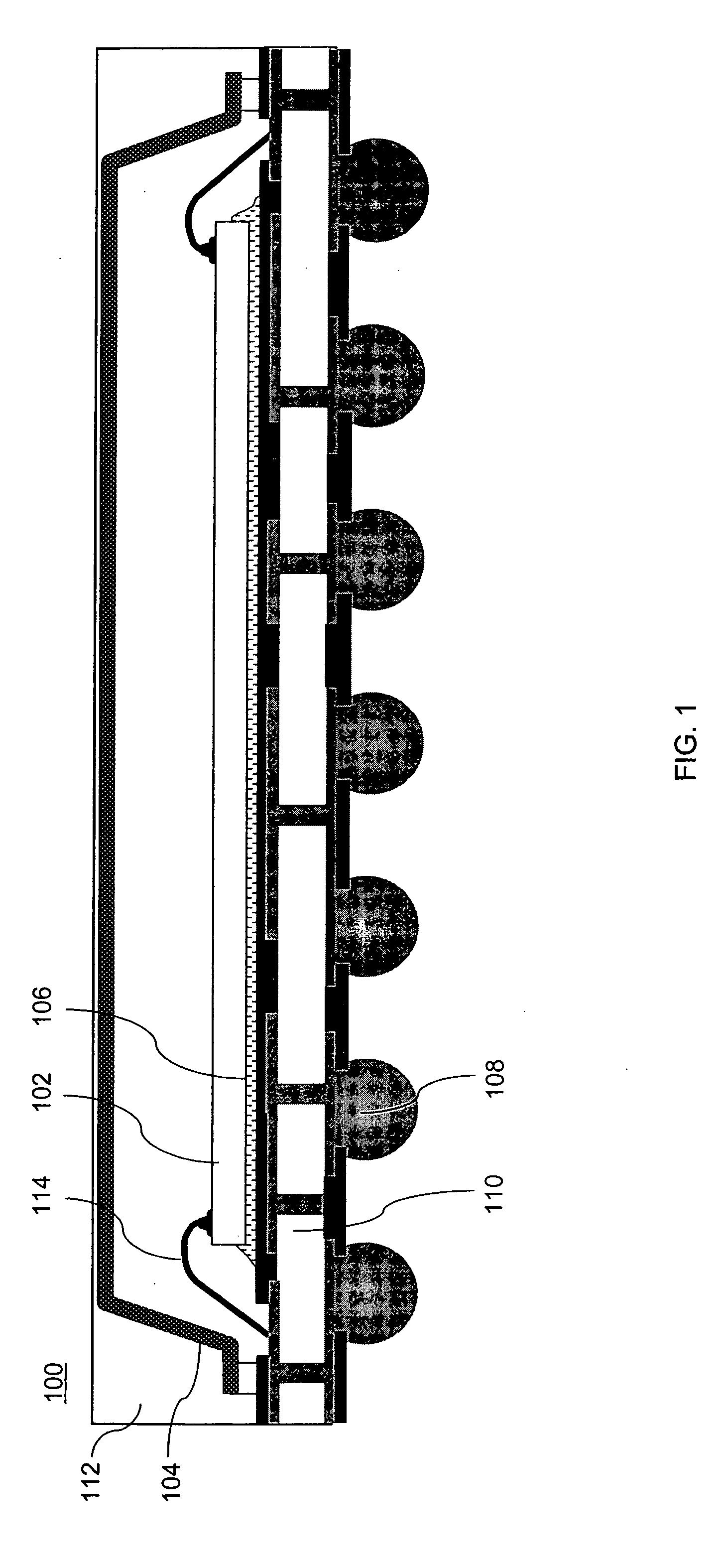
[0060]This section and the associated figures are intended to illustrate various example embodiments of the invention, but are not intended to be limiting. The following sections describe various integrated circuit (IC) package embodiments, but the invention is equally applicable to other existing or future IC device packages.

[0061]For example, FIG. 6A illustrates an example embodiment of a Plastic Ball Grid Array (PBGA) IC package 600 having an IC die 302 coupled to an interposer 310 through nodules 312. Die 302 is connected to substrate 608 by wirebond 614 and die attach material 606. Mold compound 612 encapsulates package 600, including die 302, interposer 310, wirebond 614, and all or part (e.g., a top surface) of substrate 608. Substrate 608 is configured to be connected to a printed wire board (PWB) (not shown) via solder balls 610. FIG. 6B illustrates an embodiment of a PGBA IC package 650 similar to package 600 illustrated by FIG. 6A, with the addition of underfill material ...


PUM


Abstract

A method, system, and apparatus for improved IC device packaging is described. In an aspect, an (IC) device package includes an IC die having at one or more contact pads, each contact pad located at a corresponding hotspot on a surface of the IC die. The package also includes a thermally conductive interposer which is thermally coupled to the IC die at the contact pads. In another aspect, an underfill material fills a space between the IC die and the interposer. The interposer may also be electrically coupled to the IC die. In an aspect, the interposer and the IC die are coupled through thermal interconnects or “nodules.”

Description

[0001]This application claims the benefit of U.S. Provisional Appl. No. 60 / 800,432, filed May 16, 2006, which is incorporated by reference herein in its entirety.BACKGROUND OF THE INVENTION[0002]1. Field of the Invention[0003]The invention relates generally to the field of integrated circuit (IC) device packaging technology, and more particularly to the cooling of hotspots on IC semiconductor die, heat spreading for molded plastic IC packages, and thermal interconnection technology in IC packaging.[0004]2. Background Art[0005]Electronic signals are carried by electrical current through conductors and transistors in a large scale integrated circuit (IC) fabricated on semiconductor substrate. The energy carried by the electrical current is partially dissipated along the paths of current flow through the IC in the form of heat. Heat generation in electronic semiconductor ICs is also known as power consumption, power dissipation, or heat dissipation. The heat generated, P, in an IC is t...

Claims


Application Information

Patent Timeline
IPC IPC(8): H01L23/34
CPCH01L23/3128H01L23/367H01L23/4334H01L2224/48091H01L2224/48227H01L2224/48247H01L2224/48257H01L2224/73265H01L2924/01046H01L2924/01079H01L2924/15311H01L2924/1532H01L2924/16152H01L2224/16225H01L2224/73207H01L2924/15321H01L24/48H01L2224/16145H01L2224/32225H01L2224/32245H01L2224/48228H01L2224/48465H01L2924/1815H01L2924/15153H01L2924/10253H01L2924/3025H01L2224/49109H01L2924/00014H01L2924/00H01L2924/00012H01L24/73H01L2924/14H01L2924/181H01L2224/73204H01L24/49H01L2224/45099H01L2224/45015H01L2924/207H01L21/50H01L21/563H01L23/42H01L24/16H01L2021/60262H01L2224/16238
Inventor KHAN, REZAUR RAHMANZHAO, SAM ZIQUN
Owner AVAGO TECH INT SALES PTE LTD
Why Eureka
Try Eureka