
Am Intermediate Frequency Variable Gain Amplifier Circuit, Variable Gain Amplifier Circuits and its Semiconductor Integrated Circuit

a technology of amplifier circuit and amplifier circuit, which is applied in the direction of amplification control device circuit, electric/magnetic computing, instruments, etc., can solve the problems of increasing noise inside the circuit, and achieve the effect of reducing distortion of output signals, less noise generated, and suppressing fluctuations of bias voltag

Inactive Publication Date: 2007-11-29
NSC CO LTD
View PDF6 Cites 12 Cited by
  • Summary
  • Abstract
  • Description
  • Claims
  • Application Information

AI Technical Summary

Benefits of technology

[0023] However, since the variable gain amplifier circuit 20 shown in FIG. 6 uses a larger number of MOS transistors than the variable gain amplifier circuit 10 shown in FIG. 4, noise generated inside the circuit increases. More particularly, in a variable gain amplifier circuit for amplifying an AM intermediate frequency signal, it is necessary to reduce noise in a low band.
[0024] It is an object of the present invention to provide a variable gain amplifier circuit operable with a lower power supply voltage and with less noise generated inside the circuit. It is another object of the present invention to be able to operate the gain control field-effect transistor of a variable gain amplifier circuit in a non-saturated region.

Problems solved by technology

However, since the variable gain amplifier circuit 20 shown in FIG. 6 uses a larger number of MOS transistors than the variable gain amplifier circuit 10 shown in FIG. 4, noise generated inside the circuit increases.

Method used


Image

  • Am Intermediate Frequency Variable Gain Amplifier Circuit, Variable Gain Amplifier Circuits and its Semiconductor Integrated Circuit
  • Am Intermediate Frequency Variable Gain Amplifier Circuit, Variable Gain Amplifier Circuits and its Semiconductor Integrated Circuit
  • Am Intermediate Frequency Variable Gain Amplifier Circuit, Variable Gain Amplifier Circuits and its Semiconductor Integrated Circuit

Examples


Embodiment Construction

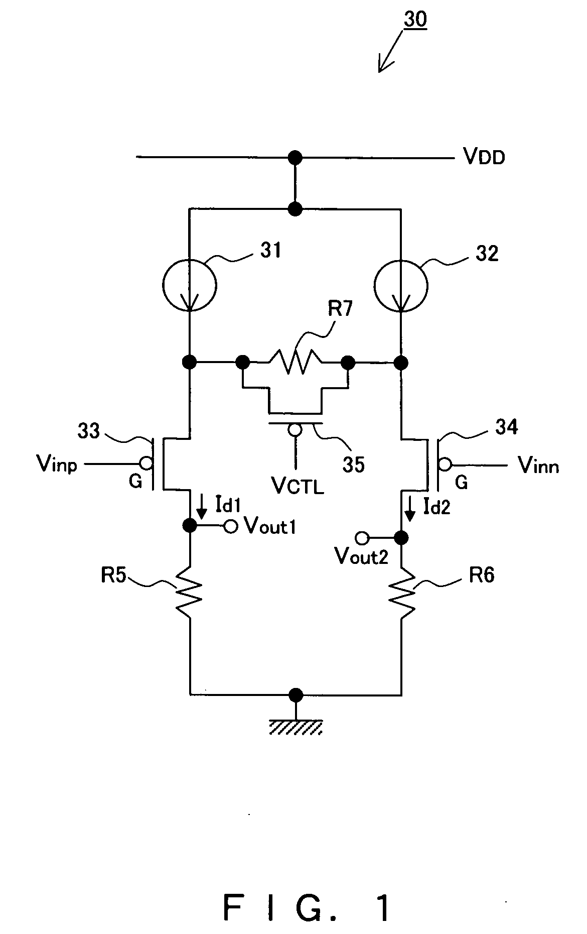
[0045] The preferred embodiments of the present invention are described below with reference to the drawings. FIG. 1 is a circuit diagram of an AM intermediate frequency variable gain amplifier circuit 30 in a first preferred embodiment of the present invention. The variable gain amplifier circuit described below is formed on a semiconductor circuit board by A CMOS process for manufacturing p-channel and n-channel MOS transistors.

[0046] In FIG. 1, one terminal of current sources 31 and 32 is connected to a power supply VDD and the other terminal is connected to the sources of p-channel MOS transistors (field-effect transistors) 33 and 34, respectively. Each of the current sources 31 and 32 comprises, for example, a current mirror circuit.

[0047] The p-channel MOS transistors 33 and 34 constitute a differential amplifier circuit, and the AM intermediate frequency signals Vinp and Vinn, whose phases differ by 180 degrees, are input to their respective gates. For the resistors R5 and ...


PUM


Abstract

It is an object of the present invention to provide a variable gain amplifier circuit operable with a low power supply voltage and with less noise generated inside the circuit. In the variable gain amplifier circuit, a third MOS transistor is connected between the respective sources of two MOS transistors constituting a differential amplifier circuit and to the gate of the third MOS transistor, and a DC bias voltage for operating the third MOS transistor in a non-saturated region is supplied. If the output voltage of an AM intermediate frequency variable gain amplifier circuit increases, a control voltage for reducing the resistance between the source and drain of the third MOS transistor is applied to reduce the gain of the AM intermediate frequency variable gain amplifier circuit.

Description

FIELD OF THE INVENTION [0001] The present invention relates to a variable gain amplifier circuit for amplifying an AM intermediate frequency signal, a variable gain amplifier circuit and a semiconductor integrated circuit mounting the variable gain amplifier circuit. BACKGROUND OF THE INVENTION [0002] A variable gain amplifier for controlling gain according to the change in level of an input signal is known in the art. As an example of the variable gain amplifier, patent reference 1 discloses a circuit in which a variable resistor means comprises a diode that is connected between the emitter terminals of a transistor constituting a differential amplifier that controls current flowing through this variable resistor means in such a way as to be proportional to the index of a control input. [0003] Patent reference 2 discloses a circuit for controlling gain by changing the resistance value of a variable resistor that has as an input the two output currents of a differential amplifier ci...

Claims


Application Information

Patent Timeline
Patent Type & Authority Applications(United States)
IPC IPC(8): H03F3/45H03G1/00H03G3/10
CPCH03G1/007H03G1/0029H03G3/10
Inventor KATSUNAGA, HIROSHIMIYAGI, HIROSHI
Owner NSC CO LTD
Features
  • Generate Ideas
  • Intellectual Property
  • Life Sciences
  • Materials
  • Tech Scout
  • Unparalleled Data Quality
  • Higher Quality Content
  • 60% Fewer Hallucinations
Learn More